Cirrus Logic AN240 User Manual
Page 2
5
5
4
4
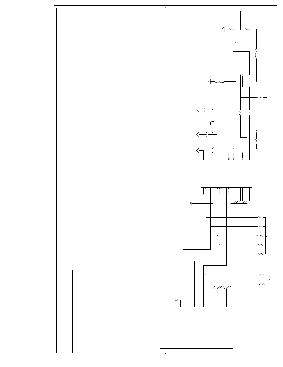
3
3
2
2
1
1
D
D
C
C
B
B
A
A
Notes:
-EP9312
symbol
i
s
incomplete
as
this
is
meant
only
for
reference
pu
rposes.
-SENSE/EOT
signal
acts
as
both
a
U
S
B
Vbus
detect
AND
t
he
end-of-transfer
signal
for
DM
A
o
p
erations.
This
is
intentional.
Please
see
the
P
hi
l
i
p
s
P
D
I
U
SBD12
datasheet
f
or
additional
d
e
t
a
i
l
s
.
-Likewise,
R10/R11
form
a
3.3V
pullup
netw
o
r
k
f
o
r
t
h
e
E
O
T
signal
v
ia
the
USB
+
5V
bus
rail.
Thus,
t
here
is
n
o
p
u
l
l
u
p
resistor
for
t
he
SENSE/EOT
s
i
g
nal.
-This
schematic
assumes
minimal
or
no
load
i
n
g
o
f
t
h
e
buses
between
the
EP9312
and
the
PDIUSBD12.
De
p
e
nding
on
your
design,
you
may
need
additional
buffer
i
n
g
t
o
r
e
d
u
c
e
the
o
verall
load
on
these
s
i
g
n
a
l
s
.
>
0
E
P
9312
U
S
B
1
.1
S
lave
B
11
T
uesday,
J
une
24,
2003
Tit
le
S
iz
e
D
o
cum
ent
N
u
m
ber
R
e
v
D
a
te
:
S
heet
of
INT1
DREQ
INT1
DA3
DA6
SEN
S
E
/E
O
T
DA5
DA7
DA7
DA6
DA1
DA4
DREQ
DA0
DA5
DA2
DA4
SEN
S
E
/E
O
T
DA2
DA1
DA0
DA3
DA[7
:0
]
VCC3
VCC3
VCC3
VCC3
VCC3
L1
FERRITE_
BEAD,
0
6
0
3
1
2
P1
USB-
B
1
2
3
4
6
5
PW
R
D-
D+
GND
SHIEL
D
SHIEL
D
R9
1.
5K
,
0603
1
2
EP9312-D
partial
SRAM
interface
U5
DA0
DA1
DA2
DA3
DA4
DA5
DA6
DA7
EG
PIO
7
/DREQ
0
EG
PIO
8
/DACK0
EG
PIO
9
/DEO
T0
INT1
/CS7
/RD
/W
R
AD0
AD1
AD2
AD3
C1
1
22P
F
,
0603
1
2
C1
2
22P
F
,
0603
1
2
R1
4.
7K
1
2
R2
4.
7K
1
2
R3
4.
7K
1
2
R1
2
4.
7K
1
2
R4
4.
7K
1
2
R7
4.
7K
1
2
X2
6M
H
Z
,
H
C
49-
U
S
1
2
R8
4.
7K
1
2
R1
1
1M
,
0603
1
2
R1
0
560K
,
0603
1
2
R
159
4.
7K
,
0603
1
2
U3
PDIUSBD1
2
,
TSSO
P
2
8
1
2
3
4
6
7
8
9
11
15
16
10
28
22
23
18
19
20
5
24
25
26
21
27
17
12
14
D0
D1
D2
D3
D4
D5
D6
D7
*CS
*RD
*W
R
AL
E
A0
XTAL
1
XTAL
2
*DMA
CK
*E
OT
*RS
T
GND
VCC
D-
D+
*GL
V3
.3
*DMRE
Q
SUSPEND
*I
NT
R5
18.
2_1%,
0603
1
2
R6
18.
2_1%,
0603
1
2
L2
FERRITE_
BEAD,
0
6
0
3
1
2