Cirrus Logic AN266 User Manual
Introduction, Implementation using gpio interrupt (for ep93xx)

1
Copyright
© Cirrus Logic, Inc. 2005
(All Rights Reserved)
http://www.cirrus.com
AN266
How to Connect NAND Flash Memory to an EP93xx
1. Introduction
This document describes two different methods that can be used to connect NAND FLASH to an EP93xx
device. The first approach takes advantage of the data bus and uses fewer GPIO pins. The second ap-
praoch uses GPIO exclusively.
2. Implementation Using GPIO Interrupt (for EP93xx)
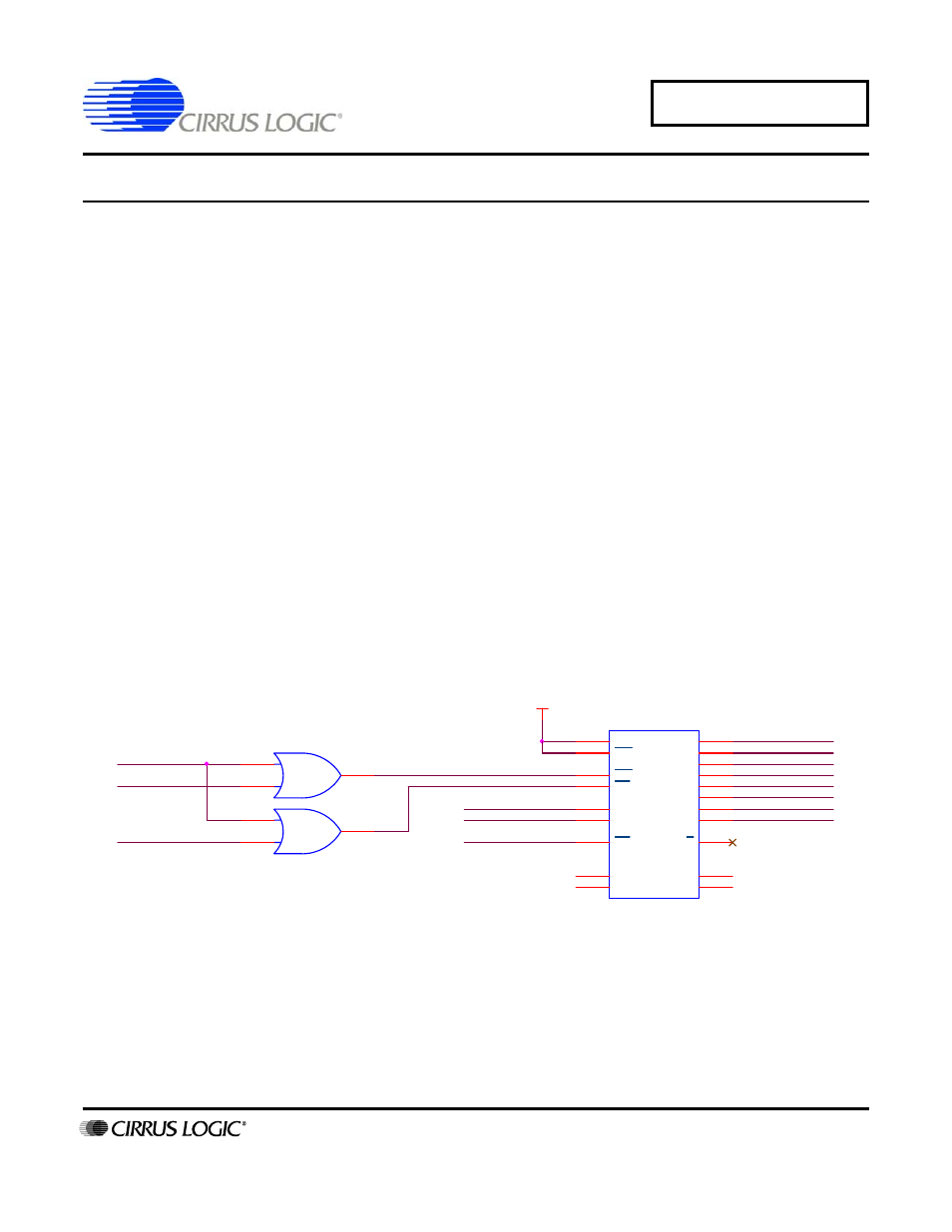
Please refer to the partial schematic below. GPIOx, GPIOy, and GPIOz may be any GPIO pins from the
EP93xx device. Not all of the devices in the EP93xx family have all of their GPIO port pins bonded out.
Refer to the datasheet for the specific device you are using. It is suggested that all the GPIO pins con-
nected to the NAND device belong to the same port for efficient code. However, this is not a requirement.
There is no GPIO signal connected to pin 7 of the NAND device in the figure below. It is not required be-
cause the ready status can be read from a bit in the Status register. If the design uses pin 7, make sure
that the GPIO line used has interrupt capability. Referring to the EP93xx User's Guide, GPIO section, you
will notice Ports A, B, and F have interrupt capability. Note that Port A and B have interrupt capability but
it is implemented as a single interrupt signal called GPIOINTR. All pins on Port F are available to the sys-
tem interrupt controller as GPIO[7:0]INTR.
The example below connects an EP93xx to the SAMSUNG K9F2G08U0M.
Figure 1. Example of Implementation Using Minimal GPIO
D1
/NAND_RE
GPIOy
D0
/WE
D5
GPIOx
1
2
3
/RE
D7
D4
/CSx
/NAND_WE
1
2
3
D3
PWR_3V3
D2
GPIOz
U2
K9F2G08
29
30
31
32
41
42
43
44
19
18
17
16
9
8
7
12
37
13
36
38
D0
D1
D2
D3
D4
D5
D6
D7
WP
WE
ALE
CLE
CE
RE
R/B
PWR_3V3
PWR_3V3
GND
GND
PRE
D6
FEB ‘05
AN266REV1
