Cirrus Logic AN339 User Manual
Introduction, Summary of improvements
Copyright
Cirrus Logic, Inc. 2009
(All Rights Reserved)
http://www.cirrus.com
AN339
CS8416 Delivers Performance Gains Over CS8413/14
by
Jonathan Schwartz
1. INTRODUCTION
The CS8413/14 S/PDIF receivers have long held a position of respect as the industry-favored receivers for recov-
ered clock quality. As of early 2009, an upcoming end-of-life of these products has many system designers wonder-
ing what their next move will be, and where they’ll go to get the level of performance they’ve become accustomed
to. Others simply need 192 kHz support, which the CS8413/14 does not provide.
Satisfying both of these requirements, Cirrus Logic offers the
CS8416 S/PDIF receiver with new features and lower recovered
clock jitter than the CS8413/14.
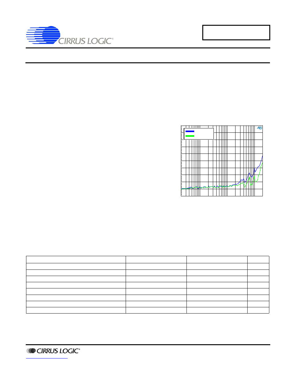
When the CS8416 was first released in 2002, it used a phase de-
tector scheme that resulted in higher recovered clock jitter com-
pared to the CS8413/14. To improve on its performance and follow
in the tradition of the CS8413/14, a new phase detector option was
added to the CS8416 in 2004. This new option offers even lower
recovered clock jitter than the CS8413/14 and results in measur-
ably improved audio performance as shown in
.
This application note details how the CS8416 improves upon the
performance of the CS8413/14. A summary of important functional
differences and detailed jitter and audio performance measure-
ments are included to clearly demonstrate the improvements that
can be expected when transitioning to the CS8416.
2. SUMMARY OF IMPROVEMENTS
Many improvements were made in the generational leap from the CS8413/14 to the CS8416. For reference, some
of the high-level improvements are summarized in the table below. For more information, please refer to each de-
vice’s datasheet.
Notes: 1.
Values listed are from experiment results. See
2.
PDUR=1. See
Parameter
CS8413/14
CS8416
Unit
Maximum Sample Rate
96
192
kHz
Baseband Jitter
158.5
122.6
ps
Logic Supply Voltage Range
5
3.3 - 5
V
Power Supply Consumption
175
47.5
mW
Back-up System Clock During Receiver Error
None
OMCK pin
-
Receiver Input Pins
1
8 in SW Mode, 4 in HW Mode
-
Dedicated Reset Pin
None
Yes
-
Control Port Protocol
Parallel Port, CS8413 Only
I²C and SPI
-
Table 1. Summary of CS8416 Improvements
-110
-90
-108
-106
-104
-102
-100
-98
-96
-94
-92
d
B
r
A
20
20k
50
100
200
500
1k
2k
5k
10k
Hz
Figure 1. DAC THD+N
CS8414
CS8416
JUL '09
AN339REV1