1 overview, Cdb5581 – Cirrus Logic CDB5581 User Manual
Page 4
CDB5581
4
DS796DB3
1.1
Overview
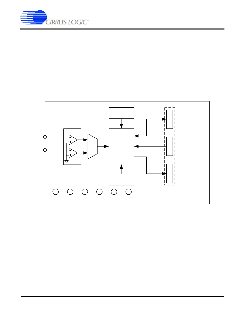
The CDB5581 evaluation board has both analog and digital circuit sections. The analog section consists
of the CS5581 ADC, two analog input signal buffers, controlled through a multiplexer, that condition the
signal into the ADC, and a precision 4.096 V reference. The digital section consists of board operation
configuration control signals, reset circuitry, an SPI™ serial port, a jumper connection for initiating ADC
calibration, and an EEPROM for evaluation board identification.
The evaluation board operates from +2.5V, -2.5V, +3.3V and communicates through an SPI™ serial port.
Figure 1 illustrates the CDB5581 block diagram.
CS5581
M
U
X
VREF
4.096 V
XTAL
16 MHz
Communication/Control
Interface
Master/Slave
Serial Port
Digital Inputs
to ADC
Digital Outputs
from ADC
IN_A
IN_B
+2.5V GND -2.5V GND +3.3V GND
J8
J6
J7
CS3004
Single-ended
Analog Inputs
Figure 1. CDB5581 Block Diagram
- CobraNet (147 pages)
- CS4961xx (54 pages)
- CS150x (8 pages)
- CS1501 (16 pages)
- CS1601 (2 pages)
- CS1601 (16 pages)
- CS1610 (16 pages)
- CRD1610-8W (24 pages)
- CRD1611-8W (25 pages)
- CDB1610-8W (21 pages)
- CS1610A (18 pages)
- CDB1611-8W (21 pages)
- CDB1610A-8W (21 pages)
- CDB1611A-8W (21 pages)
- CRD1610A-8W (24 pages)
- CRD1611A-8W (25 pages)
- CS1615 (16 pages)
- AN403 (15 pages)
- AN401 (14 pages)
- AN400 (15 pages)
- AN375 (27 pages)
- AN376 (9 pages)
- CRD1615-8W (22 pages)
- CRD1616-8W (23 pages)
- AN402 (14 pages)
- AN404 (15 pages)
- CRD1615A-8W (21 pages)
- CS1615A (16 pages)
- CS1630 (56 pages)
- AN374 (35 pages)
- AN368 (80 pages)
- CRD1630-10W (24 pages)
- CRD1631-10W (25 pages)
- CS1680 (16 pages)
- AN405 (13 pages)
- AN379 (31 pages)
- CRD1680-7W (31 pages)
- AN335 (10 pages)
- AN334 (6 pages)
- AN312 (14 pages)
- AN Integrating CobraNet into Audio Products (16 pages)
- CobraNet Audio Routing Primer (9 pages)
- Bundle Assignments in CobraNet Systems (3 pages)
- CS2300-01 (3 pages)
- CS2000-CP (38 pages)