Figure 7. power-on reset, 6 oscillator characteristics, Figure 8. oscillator connection – Cirrus Logic CS5462 User Manual
Page 12: 7 user defined settings, Cs5462, 7 user defined settings example, 26 mv
CS5462
12
DS547F1
which time the CS5462 will configure itself and re-
sume normal operation.
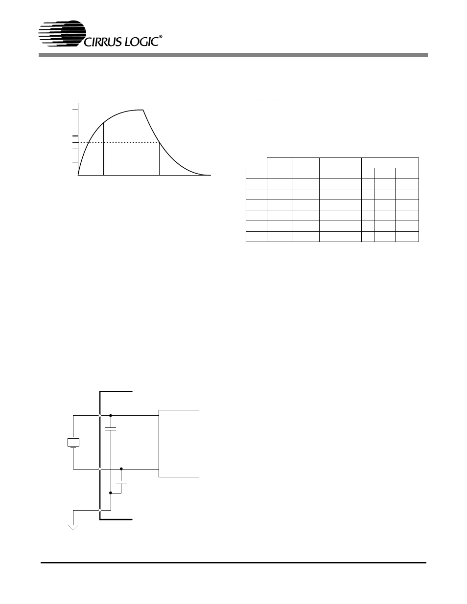
4.6
Oscillator Characteristics
XIN and XOUT are the input and output of an in-
verting amplifier which can provide oscillation and
can be configured as an on-chip oscillator, as
shown in Figure 8. The oscillator circuit is designed
to work with a quartz crystal or a ceramic resona-
tor. To reduce circuit cost, two load capacitors C1
and C2 are integrated in the device, one between
XIN and DGND, one between XOUT and DGND.
Lead lengths should be minimized to reduce stray
capacitance. To drive the device from an external
clock source, XOUT should be left unconnected
while XIN is driven by the external circuitry. There
is an amplifier between XIN and the digital section
which provides CMOS level signals. This amplifier
works with sinusoidal inputs so there are no prob-
lems with slow edge times.
4.7
User Defined Settings
EXAMPLE:
Design a hybrid stepper motor meter
with an 2 Hz maximum pulse output frequency on
the E1, E2 pins with 500 mV
P-P
signal on the in-
puts of the current and voltage channels and the
high pass filter enabled on the current channel on-
ly. Using the figure below these settings can be se-
lected with two connections.
By directly connecting FREQ with P4 and IGAIN
with P5 the CS5462 is configured to drive a step-
per motor with a maximum pulse output rate of
2 Hz, to support an input range of 500 mV
P-P
, and
to remove all DC content on the current signals by
enabling the HPFs on the Ich. The CS5462 is now
ready for calibration.
Before applying power to the chip, connect the
CAL0 and CAL1 pins to P4. This will select
0% + 0% = 0% gain adjustment. After making this
connection the CS5462 is ready to be calibrated.
Once power is applied the CS5462 will begin a
startup sequence in which it will scan the FREQ,
IGAIN, CAL0, and CAL1 pins. After determining
which connections are made the FREQ, IGAIN,
CAL0, and CAL1 pins will become high impedance
inputs and the part will begin normal operation and
start converting. If on-chip calibration is required
place known voltages across the inputs on IIN±
and VIN±.
For example, 150 mV
RMS
= ~424.26 mV
P-P
will be
used for both the current and voltage inputs.
424.26 mV
P-P
is ~84.853% of the maximum full
scale input of both the current and voltage chan-
nels. With this input on both channels the expected
pulse output frequency is
84.853% * 84.853% = 72% of full scale. This
Reset
Reset
Normal
Operation
5 V
4 V
2.5 V
1 V
0 V
Time
Supply
Voltage
Figure 7. Power-on Reset
Oscillator
Circuit
DGND
XIN
XOUT
C1
C1 =
22 pF
C2
C2 =
Figure 8. Oscillator Connection
P1
P2
P3
P4
P5
P6
P7
10x
50x
10x
50x
50x
10x
10x
CAL1
CAL0
0.25 Hz (stp)
FREQ
+4.2%
+2.8%
+1.4
0
-1.4%
-2.8%
-4.2%
IGAIN
+0.6%
+0.4%
+0.2%
0
-0.2%
-0.4%
-0.6%
0.5 Hz (stp)
1 Hz (stp)
2 Hz (stp)
4 Hz (stp)
4 Hz (mc)
16 Hz (mc)
500mV
100mV
500mV
100mV
100mV
500mV
500mV
no hpf
no hpf
hpf both
hpf both
hpf Ich
hpf Vch
hpf Ich
Figure 9. Calibration, Frequency Select, and
PGA Select