1 order of calibration sequences, An227 – Cirrus Logic AN227 User Manual
Page 2
AN227
2
taneous Current Register) will be obtained when-
ever the input voltage across the IIN+ and IIN- pins
is 187.5 mV (DC). Note that this level is ~75% of
the (typical) maximum available input voltage
range [i.e, ~
±
250 mV DC.] In this situation, the cur-
rent channel input ranges for which ±0.1% linearity
+ variation are guaranteed will be reduced to be-
tween 0.5 mV (DC) and 187.5 mV (DC), as op-
posed to what is specified in Table 1 [which would
translate into a voltage range between 0.5 mV
(DC) and 250 mV (DC)].
Also note that using gain calibration signal levels
which cause the CS5460A to set the internal gain
registers to a value that is less than unity will effec-
tively decrease the guaranteed “±0.1% of reading”
linearity+variation range (and therefore the accura-
cy range) of the RMS calculation results and the
overall energy results. This will occur whenever a
DC gain calibration is performed (on either chan-
nel) of a CS5460A sample while applying a DC sig-
nal whose value is less than the individual
sample’s inherent maximum differential DC input
voltage level. This will also occur whenever an AC
gain calibration is performed (on either channel)
using an AC signal whose RMS value is less then
60% of the sample’s inherent maximum AC input
voltage levels.
Finally, remember that the ±0.1% (of reading) ac-
curacy guarantee is made with the assumption that
the device has been calibrated with MCLK =
4.096 MHz, K = 1, and N = 4000. If MCLK/K be-
comes too small, or if N is set too low (or a combi-
nation of both), then the CS5460A may not exhibit
±0.1% linearity + variation.
1.1 Order of Calibration Sequences
Should offset calibrations be performed before
gain calibrations? Or vice-versa? This section
summarizes the recommended order of calibra-
tion.
1. If the user intends to measure any DC content
that may be present in the voltage/current and
power/energy signals, then the DC offset calibra-
tion sequences should be run (for both channels)
before any other calibration sequences. However if
the user intends to remove the DC content present
in either the voltage or current signals (by turning
on the voltage channel HPF option and/or the cur-
rent channel HPF option--in the Status Register)
then DC offset calibration does not need to be ex-
ecuted for that channel. Note that if either the volt-
age HPF or current HPF options are turned on,
then any DC component that may be present in the
power/energy signals will be removed from the
CS5460A’s power/energy results.
2. If the user intends to set the energy registration
accuracy to within ±0.1% (with respect to reference
calibration levels on the voltage/current inputs)
then the user should next execute the gain calibra-
tions for the voltage/current channels. The user
can execute either the AC or DC gain calibration
sequences (for each channel).
3. Finally, the user should (if desired) run the AC
offset calibration sequences for the voltage and
current channels. Simply ground the “+” and “-” in-
puts of both channels and execute the AC offset
calibration sequence.
Note that technically, by following the order of cal-
ibrations as suggested above, if DC offset calibra-
tion is performed for a given channel, and
afterwards a gain calibration is performed on the
channel, then the DC offset register value for the
channel should be scaled by a factor equal to the
respective channel’s new gain register value. For
example, suppose that execution of DC offset cal-
ibration for the voltage channel results in a value of
0x0001AC = 0.0000510(d) in the Voltage Channel
DC Offset Register (and we assume that the value
in the Voltage Channel Gain Register was at its de-
fault value of 1.000... during execution of this DC
offset calibration). Then if AC or DC gain calibra-
tion is executed for the voltage channel such that
the Voltage Channel Gain Register is changed to
0x4020A3(h) = 1.0019920(d), then the user may
want to modify the value in the Voltage Channel
Energy
Vrms
Irms
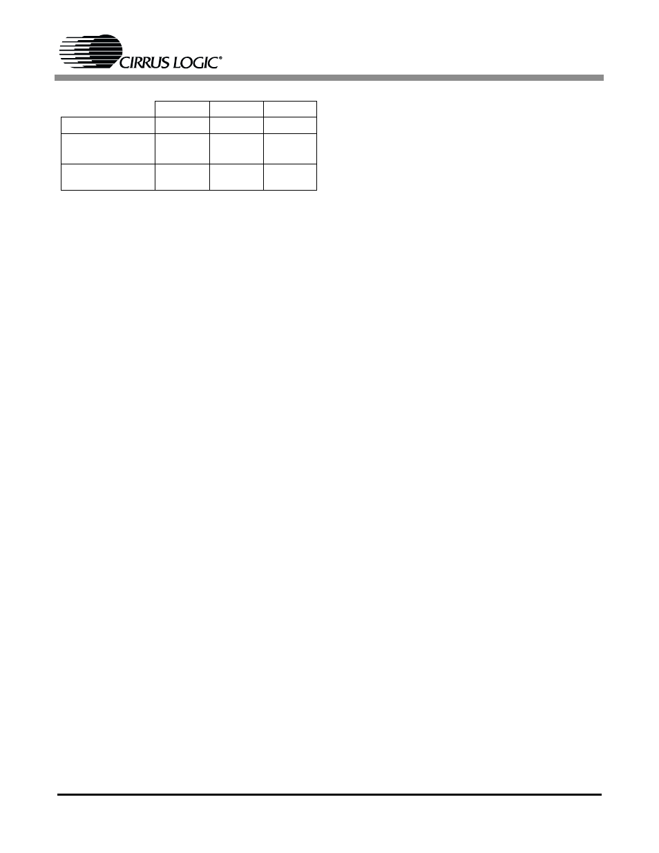
Range (% of FS)
0.1% - 100%
50% - 100%
0.2% - 100%
Max. Differential
Input
not applicable
V-channel:
±250 mV
I-channel:
±250 mV 10x
±50 mV
50x
Linearity
0.1% of
reading
0.1% of
reading
0.1% of
reading
Table 1. Available range of ±0.1% output linearity, with
default settings in the gain/offset registers.