Cdb5364 hardware, 1 input and output connectors, Table 1. cdb5364 input and output connectors – Cirrus Logic CDB5364 User Manual
Page 9

DS625DB1
9
CDB5364
In TDM mode, SDOUT_SEL1 and SDOUT_SEL 0 extract two stereo pairs from the CS5364 TDM stream,
convert the data to Left-Justified PCM format and send the data to the CS8406 data input pin.
0x00 TDM Pair 1 (Channel 1, 2)
0x01 TDM Pair 2 (Channel 3, 4)
0x1x Reserved
In PCM mode, SDOUT_SEL1 and SDOUT_SEL 0 select which SDOUT pin of the CS5364 is sent to the
CS8406.
0x00 SDOUT1 (Channel 1, 2)
0x01 SDOUT2 (Channel 3, 4)
0x1x Reserved
TDM2PCM/PCM selects the clock source for the CS8406.
0x00 8406 Clock Source is CS5364
0x01 8406 Clock Source is the FPGA TDM2PCM engine
4. CDB5364 HARDWARE
The CDB5364 Evaluation Board has a number of connections, switches and jumpers that provide ease and conve-
nience for quickly evaluating the most commonly used functions of the CS5364 silicon device. The following tables
list the purpose of each hardware option on the Evaluation Board.
4.1
Input and Output Connectors
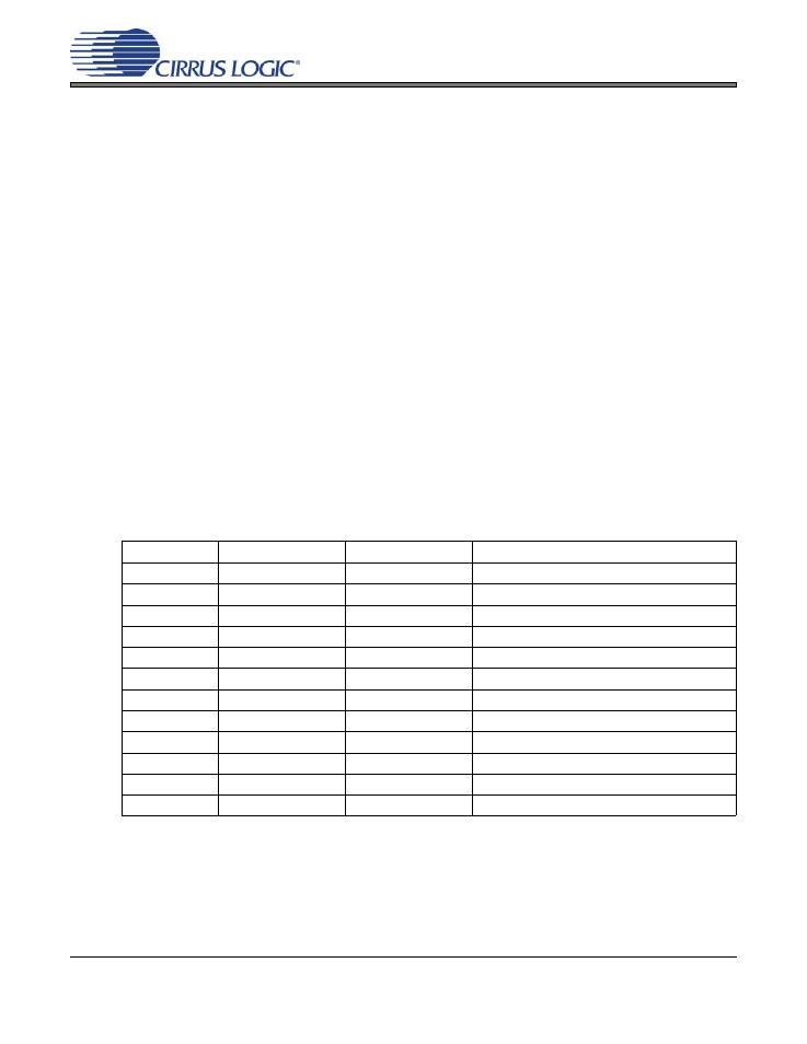
The input and output connectors provide power and signal connectivity to the CDB5364 Evaluation Board
as shown in
.
Table 1. CDB5364 Input and Output Connectors
DESIGNATOR
NAME
CLASS
FUNCTION
J6
GND
Ground
Ground connection from power supply
J2
+5 V
Power
+ 5 Volt power for CS5364
J16
+12 V
Power
+12 V power for the active input buffers
J17
-12 V
Power
-12 V power for the active input buffers
J20
AIN1
Analog Input
Analog input channel 1
J21
AIN2
Analog Input
Analog input channel 2
J22
AIN4
Analog Input
Analog input channel 4
J23
AIN3
Analog Input
Analog input channel 3
OPT1
Optical Output
Digital Output
S/PDIF Optical Digital audio output
J3
Coax Output
Digital Output
S/PDIF Coaxial Digital audio output
J5
RS232 I/O
Digital I/O
FlexGUI Interface port to PC
J10
USB I/O
Digital I/O
FlexGUI Interface port to PC
