Cirrus Logic AN239 User Manual
Analog input buffer design, By kevin l tretter

1
Copyright
Cirrus Logic, Inc. 2003
(All Rights Reserved)
www.cirrus.com
AN239
CS5361/CS5381 Compatibility
by Kevin L Tretter
1. Analog Input Buffer Design
1.1
Introduction
There are many considerations that must be taken into account when designing and implementing an an-
alog input buffer. These include negligible noise contribution, input biasing, isolation from switched ca-
pacitor currents, maintaining a low output impedance so as not to cause distortion, and providing anti-
alias filtering appropriate for the modulator sample rate.
1.2
Recommended Differential Input Buffer
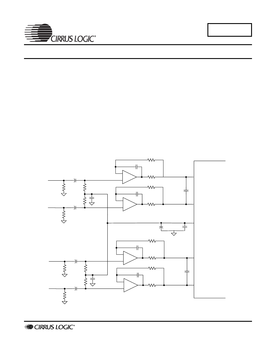
Figure 1 shows the recommended fully differential input buffer for the CS5361 and CS5381. This input
buffer will work well with both devices. However, if full performance is to be realized, then care must be
taken when selecting the op amps to ensure that the noise level of the input buffer is insignificant relative
to the converter. The CDB5361 and CDB5381 implement the NE5532 op amp, which provides an ade-
quate noise floor to see full performance from these two converters.
Figure 1. Recommended Differential Input Buffer for the CS5361 and CS5381
AIN+
AIN-
VQ
-
+
-
+
470 pF
C0G
470 pF
C0G
CS5361/CS5381
634
Ω
91
Ω
634
Ω
91
Ω
2700 pF
C0G
10
µF
10
µF
10 k
Ω
10 k
Ω
0.01
µF
1
µF
0.01
µF
100 k
Ω
100 k
Ω
-
+
-
470 pF
C0G
470 pF
C0G
634
Ω
91
Ω
634
Ω
91
Ω
2700 pF
C0G
10
µF
10 k
Ω
10 k
Ω
0.01
µF
100 k
Ω
AIN+
AIN-
100 k
Ω
10
µF
+
-
NE5532
NE5532
NE5532
NE5532
MAY ‘03
AN239REV1
