Cdb5340 – Cirrus Logic CDB5340 User Manual
Page 4
CDB5340
4
DS601DB1
* denotes default factory settings
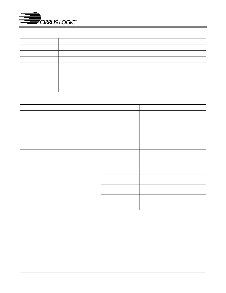
CONNECTOR
INPUT/OUTPUT
SIGNAL PRESENT
VA/VD
Input
+3.3V to +5V power for the CS5340
VL
Input
+2.5V to +5V power for the CS5340
GND
Input
Ground connection from power supply
+5V
Input
+ 5 Volt power
AINL
Input
Analog input left channel
AINR
Input
Analog input right channel
Optical Output
Output
Digital audio output
Coax Output
Output
Digital audio output
Table 1. System Connections
JUMPER/SWITCH
PURPOSE
POSITION
FUNCTION SELECTED
J5
VA/VD Power Source
ADJ
*+3.3V
+5V
Power from the Binding Post (J1)
Power from the +3.3V Regulator
Power from the +5V Supply
J6
VL Power Source
ADJ
*+3.3V
+5V
Power from the Binding Post (J2)
Power from the +3.3V Regulator
Power from the +5V Supply
J11
Input/Output for
clocks/data
-
-
S1
Reset for the CDB5340
-
-
S2
CDB5340 Configuration
M1/M0
Open
*Closed
Hi
Low
SCLK/LRCK Open
*Closed
Header J11 is an input for clocks.
Header J11 is an output for clocks.
MCLK
Open
*Closed
Header J11 is an input for MCLK.
Header J11 is an output for MCLK.
8406
Open
*Closed
CS8406 in Master mode
CS8406 in Slave mode
DIF
Open
*Closed
Digital interface format set to I
2
S
Digital interface format set to
Left Justified
Table 2. CDB5340 Jumper and Switch Settings