Cirrus Logic CDB4955A User Manual
Preliminary product information, Features, Description

Preliminary Product Information
This document contains information for a new product.
Cirrus Logic reserves the right to modify this product without notice.
1
Copyright
Cirrus Logic, Inc. 2001
(All Rights Reserved)
P.O. Box 17847, Austin, Texas 78760
(512) 445 7222 FAX: (512) 445 7581
http://www.cirrus.com
CDB4954A/55A
Evaluation Board for CS4954/55
Features
l
Demonstrates recommended layout and
grounding practices
l
Supports both parallel and serial digital
video input
l
On-board test pattern generation
l
Supports NTSC/PAL video formats
l
3.3 V or 5 V operation
l
Composite, S-Video, and RGB outputs
l
Supports Standalone mode via onboard
DIP switch
l
RS232 interface with PC
l
Single 6-9 V external DC power supply
l
Additional op-amps with open pads for
prototyping additional filters
Description
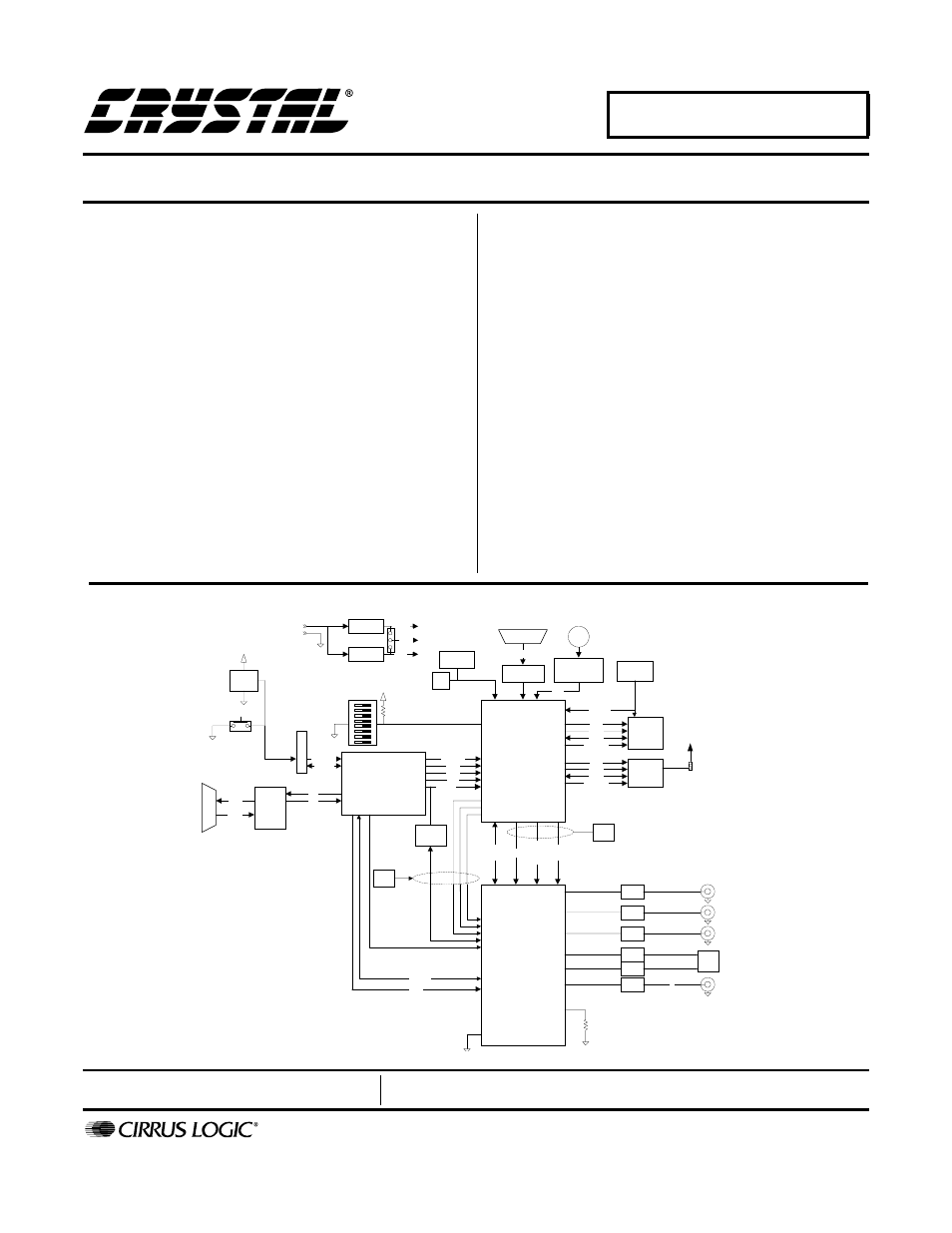
The CDB4954A/55A board allows fast evaluation of the
features of the CS4954 digital video encoders. The
board may also be configured to accept external TTL
level timing and data signals for use during system
development.
Also, to simplify the demonstration of the features of the
CS4954, the CDB4954A/55A is equipped with an on-
board microcontroller and pre-programmed FLASH
memory to facilitate configuration and evaluation of the
CS4954 digital video encoder.
ORDERING INFORMATION
CDB4954A
Evaluation Board
CDB4955A
Evaluation Board
I
Regulator
Motorola 908
Microcontroller
+3.3V
+5V
Reset
FPGA
A/D7:0
CS4954
SDRAM
SCL
SDA_O
DB25
Reset
Switch
Data
CTL
656
DATA
/8
HS,VS,
FIELD
TTX
/2
OSC
54MHZ
4K
1%
ADDR
RD-
WR-
DAT<7..0>
RST-
TTXD,
TTXRQ
ALE
OUT
FILT
OUT
FILT
OUT
FILT
OUT
FILT
OUT
FILT
OUT
FILT
u
Addr
RX
TX
ECL
RECEIVER
656_IN
D
B
9
RS-232
Interface
TXD
RXD
R
G
B
Y
C
CVBS
27MHz
PLD
EEPROM
ISP
WR-
RD-
TEST
SCL
SDA
POWER
INLET
6.5 - 10VDC
1
2
3
4
5
6
7
8
OPE
N
Hdr -
16PIN
SD
L
SD
A
Regulator
3.3V
or
+5V
BNC
SMPTE-259M
Interface
656
Flash
245
BUFFER
RESET-
Hdr -
16PIN
RESE
T
RESET-
Data
CTL
Addr
RESET-
RCA
CONNECTORS
DIN4
CONN.
RCA
CONNECTOR
PROG
MPU
PROGRAM
HEADER
RESET-
PROGRAMMING
ENABLE
JUMPER
SELECTABLE
HI/LOW
IMPEDANCE
FILTERS
CCIR 656 SERIAL/ PARALELL
INPUTS
PC SERIAL
INTERFACE
MAY ‘01
DS278DB2
Document Outline
- Features
- Description
- 1. CDB4954A/55A System Overview
- 2. SetUP Activities
- 3. Command Line Parameters
- 4. 3.3 V OR 5 V Interface
- 5. Digital video interface
- 6. Analog Output
- 7. Output filters
- Figure 3. 300 W Filters
- Figure 4. 75 W Filters
- Table 1. System Connections
- Table 2. CBD4954 Jumper/Switch Settings
- Table 3. DIP Switch Settings
- Figure 5. Digital Video Input
- Figure 6. FPGA
- Figure 7. CS4954/5
- Figure 8. Microprocessor
- Figure 9. Video Output Filters
- Figure 10. Power/RS232 Interface
- Figure 11. Silkscreen Top
- Figure 12. Top Side
- Figure 13. Power Layer
- Figure 14. Ground Layer
- Figure 15. Bottom Side
