2 transitioning from the cs4382 to cs4385, 1 hardware changes, An259 – Cirrus Logic AN259 User Manual
Page 4: Cs4382, Cs4385
AN259
4
AN259REV2
alog filter gain (if similar output level to the CS4382 is desired).
-
The mute control pins are high impedance while reset is asserted. An external pull-up or down is
required to properly bias the off-chip mute circuit into muting during reset.
-
The dual serial port function of the CS4382 which accepted two simultaneous synchronous sam-
ple rates (such as 192 kHz front and 96 kHz surrounds) is not supported.
2.2
Transitioning from the CS4382 to CS4385
2.2.1
Hardware changes
The CS4385 pinout was primarily based on the CS4382 with only 3 pins changing function. Other pins
have new recommended components but the circuit topologies remain the same and thus do not
require modification to the PCB. The most significant change is that the VD core of the CS4385
requires 2.5 V for operation, whereas the CS4382 was able to run from 3.3 V to 5 V. The CS4385 will
NOT operate off of a VD supply of 3.3 V or 5 V.
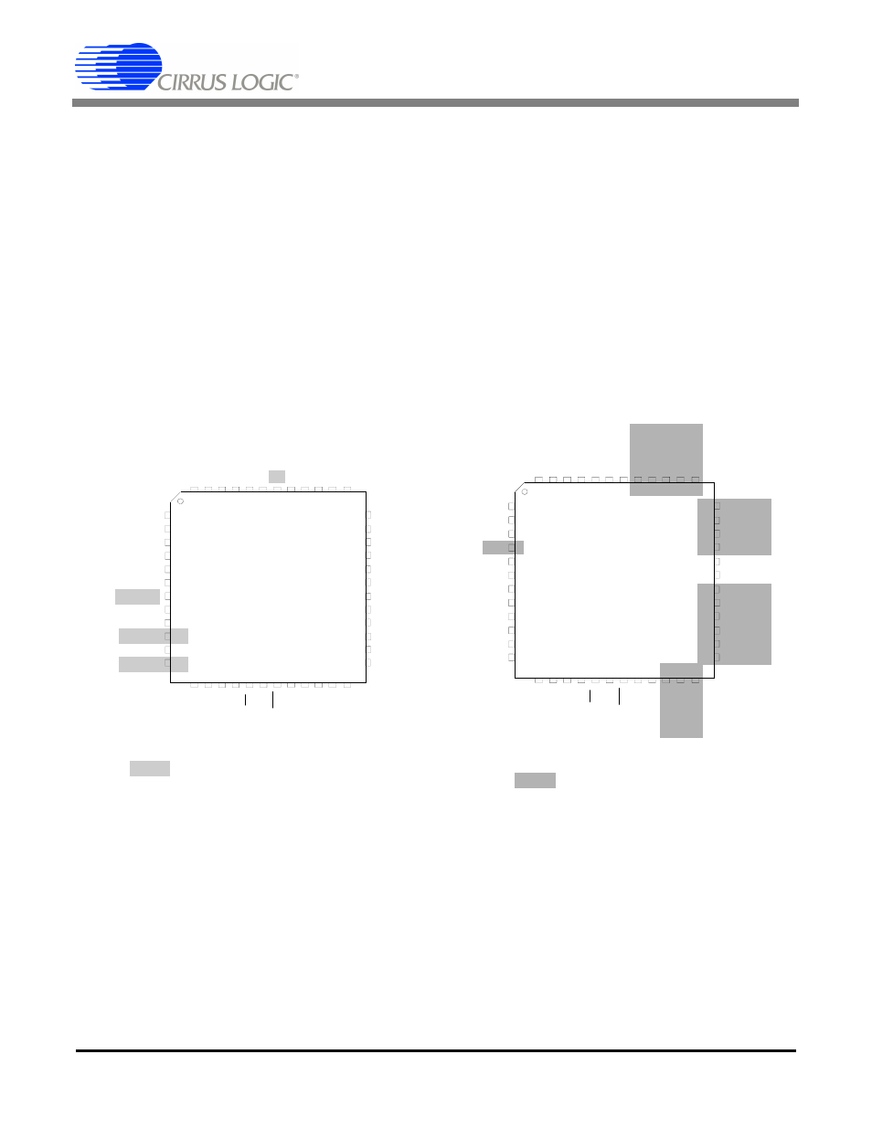
Figure 3 and Figure 4 show the CS4382 and CS4385 pinouts respectively. The changes to the two
pinouts are highlighted. Figure 3 highlights the pins which have changed function and which may
require a PCB change. Figure 4 highlights the pins which have new recommended components.
Location or function changes as denoted in Figure 3 are as follows:
•
Pin 7 is no longer DSD_EN in hardware mode. In order to enter DSD mode on the CS4385 you must either
set the M4 and M3 pins accordingly or use SPI™ or I
2
C configuration.
•
The CS4385 does not support the simultaneous synchronous sample rate function of the CS4382. Pins 10
and 12 are now dedicated for stand-alone configuration (voltage input on these pins are still referenced to
VLS).
•
Pin 42 no longer functions as M3 in stand-alone PCM modes. It is now a dedicated DSD_SCLK pin.
SDI
N
3
GND
AOUTB2-
AOUTA3+
AOUTB3-
AOUTB2+
VA
AOUTA3-
AOUTB3+
6
2
4
8
10
1
3
5
7
9
11
12
13 14 15 16 17 18 19 20 21 22 23 24
31
35
33
29
27
36
34
32
30
28
26
25
48 47 46 45 44 43 42 41 40 39 38 37
MCLK
DSDB1
VD
SDIN1
LRCK2
DSDA2
DSDA1
GND
SCLK1
SDIN2
SCLK2
LRCK1(DSD_EN)
M3(D
SD
_S
CLK
)
DSD
B
3
DSD
A
3
DSD
A
4
CS4382
DSD
B
4
VLS
SDI
N
4
M2(S
CL/
C
CL
K)
M
1
(S
DA
/C
DIN
)
VLC
RS
T
FIL
T
+
VQ
MU
T
E
C
234
M0
(A
D
0
/C
S
)
AOUTA2+
AOUTA2-
AO
UT
B
1
+
AOU
T
B
1
-
AOU
T
A
1
-
AO
UT
A
1
+
DS
DB
2
MUT
E
C1
AOUTA4-
AOUTA4+
AO
UTB
4
+
AO
UTB
4
-
= denotes location or function changes
when trasitioning to CS4385
Figure 3. CS4382 pinout
SDIN
3
GND
AOUTB2-
AOUTA3+
AOUTB3-
AOUTB2+
VA
AOUTA3-
AOUTB3+
AOUTA4-
AOUTA4+
6
2
4
8
10
1
3
5
7
9
11
12
13 14 15 16 17 18 19 20 21 22 23 24
31
35
33
29
27
36
34
32
30
28
26
25
48 47 46 45 44 43 42 41 40 39 38 37
MCLK
DSDB1
VD
SDIN1
M4
DSDA2
DSDA1
GND
SCLK
SDIN2
M3
LRCK
DS
D
_
S
C
L
K
DS
DB3
DS
DA3
DSD
A
4
CS4385
DSD
B
4
VL
S
SDIN4
M2
(S
CL
/C
CL
K)
M1(S
DA/CDIN
)
VLC
RST
FI
L
T
+
VQ
M
U
T
E
C234
AOUTB4-
AOU
T
B
4
+
M0
(A
D0
/C
S)
AOUTA2+
AOUTA2-
AOU
T
B
1
+
AOU
T
B
1
-
AO
U
T
A
1
-
AO
U
T
A
1
+
DSD
B
2
MUTEC1
= denotes pins which require changes
to components or voltages
Figure 4. CS4385 pinout