2 functional changes, Figure 1 and, Gure 2 show the cs4 – Cirrus Logic AN260 User Manual
Page 3: Gure 1, E. figure 2 h, An260, Cs4362a, Cs4362
AN260
AN260REV2
3
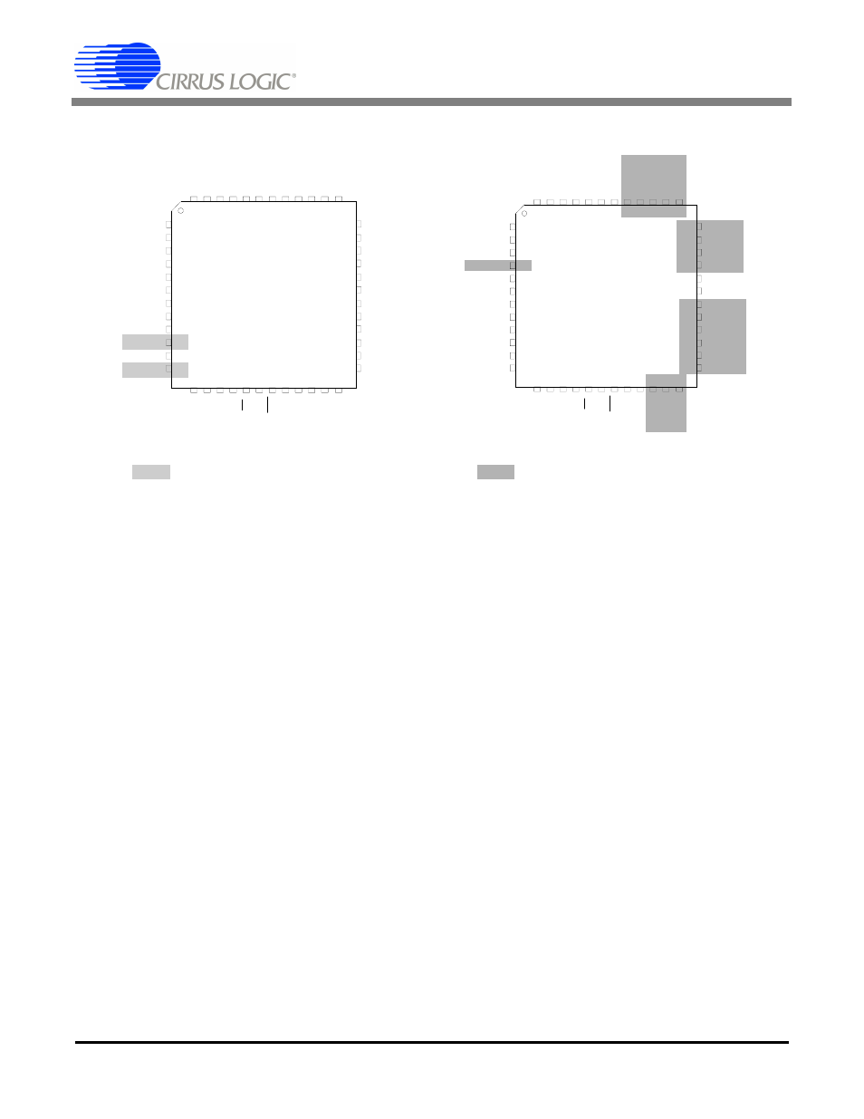
Location or function changes as denoted in Figure 1 are as follows:
•
The CS4365 does not support the simultaneous synchronous sample rate function of the CS4362. Pins 10
and 12 are now Test inputs.
Pins which require changes to external components or voltages as denoted in Figure 2 are as
follows:
•
Pin 4 (VD) requires 2.5 V for recommended operation. The CS4362 used either 3.3 V or 5 V, which, if left
unchanged, would damage the CS4362A.
•
Pins 22-26 and pin 41 (MUTEC#) require an additional pull-up or down in order to mute during reset. While
reset is asserted these pins are high impedance and will not drive the mute circuitry. It is recommended that
the pull-up/down resistance properly biases the off-chip mute circuit into muting.
•
Pins 27 - 30, 33 - 40 (AOUTs) have a new recommended filter circuit. This filter uses the same filter topology
as the CS4362. The component values have been changed to account for the extra output level from the
CS4362A and still provide 2 Vrms on the output. A general optimization was also made in order to reduce
the thermal noise contribution of the resistances (using smaller resistances where possible). Please refer to
the CS4362A datasheet for details on the new recommended filter.
2.1.2
Functional changes
-
With the addition of the non-decimating DSD processor mode comes the added benefits of
matched PCM and DSD output levels and an on chip 50 kHz filter.
-
The CS4362A uses a new multi-bit Delta-Sigma modulator core with mis-match shaping which al-
lows for lower over-all out-of-band noise and improved audio quality.
-
The CS4362A gained new digital filters with improved stop-band performance and lower latency.
-
The full-scale differential output voltage has increased which needs to be accounted for in the an-
Figure 1. CS4362 pinout
SD
IN3
GND
AOUTB2-
AOUTA3+
AOUTB3-
AOUTB2+
VA
AOUTA3-
AOUTB3+
6
2
4
8
10
1
3
5
7
9
11
12
13 14 15 16 17 18 19 20 21 22 23 24
31
35
33
29
27
36
34
32
30
28
26
25
48 47 46 45 44 43 42 41 40 39 38 37
MCLK
DSDB1
VD
SDIN1
TST
DSDA2
DSDA1
GND
SCLK1
SDIN2
TST
LRCK1(DSD_EN)
M3
(D
S
D
_S
CL
K
)
DS
DB
3
DS
DA
3
TS
T
CS4362A
TS
T
VLS
TS
T
M2
(SC
L
/C
CLK
)
M1
(S
D
A
/C
DI
N)
VL
C
RS
T
FI
LT
+
VQ
MUT
E
C
6
M0
(A
D0
/C
S
)
AOUTA2+
AOUTA2-
AO
U
T
B
1
+
AOU
T
B
1
-
AO
UTA1-
AOU
T
A1
+
DSD
B
2
MU
TE
C1
MUTEC2
MUTEC3
MU
TEC
4
MU
TEC
5
= denotes pins which require changes
to components or voltages
Figure 2. CS4362A pinout
SDI
N
3
GND
AOUTB2-
AOUTA3+
AOUTB3-
AOUTB2+
VA
AOUTA3-
AOUTB3+
6
2
4
8
10
1
3
5
7
9
11
12
13 14 15 16 17 18 19 20 21 22 23 24
31
35
33
29
27
36
34
32
30
28
26
25
48 47 46 45 44 43 42 41 40 39 38 37
MCLK
DSDB1
VD
SDIN1
LRCK2
DSDA2
DSDA1
GND
SCLK1
SDIN2
SCLK2
LRCK1(DSD_EN)
M3
(D
SD
_
S
CL
K
)
DS
DB
3
DS
DA
3
TST
CS4362
TST
VL
S
TST
M
2
(S
CL
/CCL
K)
M1
(S
DA/CDIN
)
VL
C
RS
T
FIL
T
+
VQ
MUTE
C6
M0
(A
D0
/C
S
)
AOUTA2+
AOUTA2-
AO
UT
B
1
+
AO
UT
B1
-
AO
UT
A1
-
AO
UT
A1+
DS
DB2
MUTE
C1
MUTEC2
MUTEC3
MUTE
C4
MUTE
C5
= denotes location or function changes
when trasitioning to CS4362A