Cirrus Logic CDB435 User Manual
Cdb4352, Evaluation board for cs4352, Cs4352
Copyright
© Cirrus Logic, Inc. 2006
(All Rights Reserved)
Evaluation Board for CS4352
Features
Demonstrates Recommended Layout And
Grounding Arrangements
CS8416 Receives S/PDIF, & EIAJ-340-
Compatible Digital Audio
Headers for External PCM Audio
Requires Only a Digital Signal Source and
Power Supplies for a Complete Digital-to-
Analog Converter System
Description
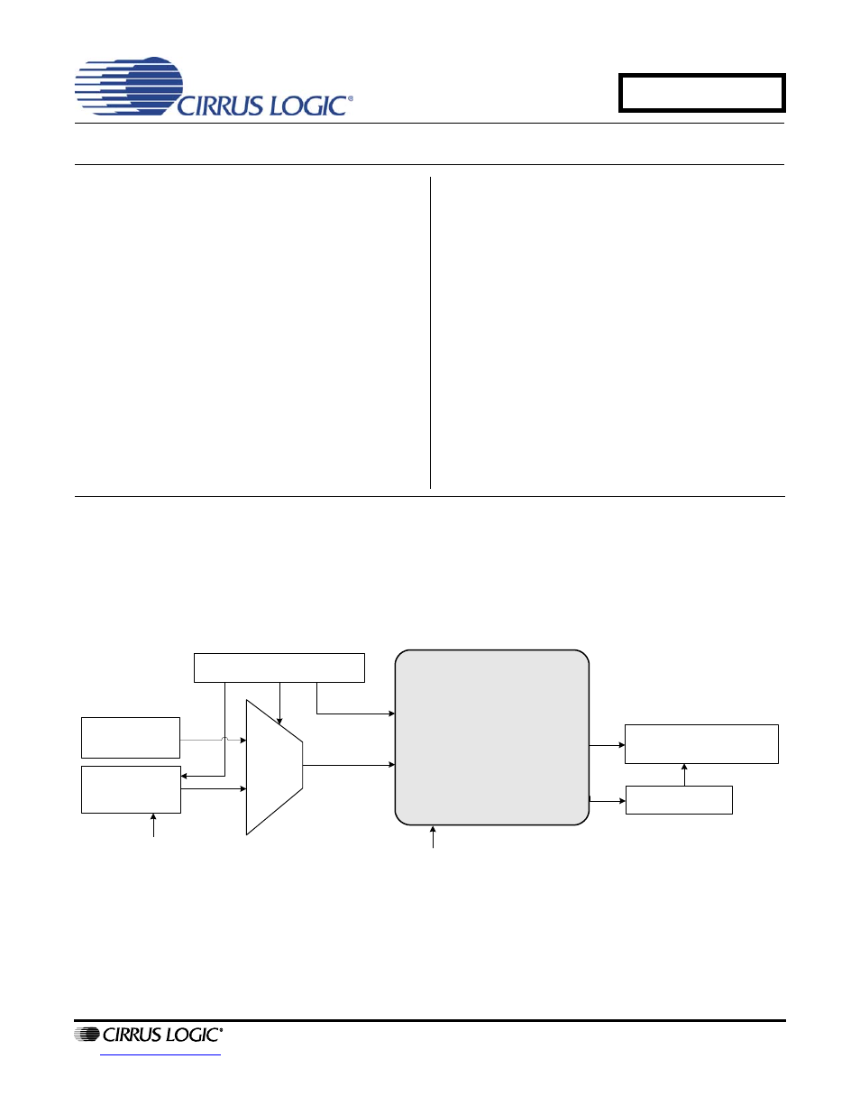
The CDB4352 evaluation board is an excellent means
for quickly evaluating the CS4352 24-bit, high-perfor-
mance stereo D/A converter. Evaluation requires an
analog signal analyzer, a digital signal source, and a
power supply. Analog line-level outputs are provided via
RCA phono jacks.
The CS8416 digital audio receiver IC provides the sys-
tem timing necessary to operate the Digital-to-Analog
converter and will accept S/PDIF and EIAJ-340-com-
patible audio data. The evaluation board may also be
configured to accept external timing and data signals for
operation in a user application during system
development.
ORDERING INFORMATION
CDB4352
Evaluation Board
Analog Output
(Line Level)
CS4352
S/PDIF Input
(CS8416)
Clocks/Data
Header
Reset
Reset
Hardware Switches
Mux
Muting
SEPTEMBER '06
DS684DB1
CDB4352
Document Outline
- 1. CDB4352 System Overview
- 2. CS4352 Digital-to-Analog Converter
- 3. CS8416 Digital Audio Receiver
- 4. Input for Clocks and Data
- 5. Power Supply Circuitry
- 6. Grounding and Power Supply Decoupling
- 7. Hardware Control
- 8. Analog Output Filtering
- 9. Performance Plots
- Figure 1. FFT (48 kHz, 0 dB)
- Figure 2. FFT (48 kHz, -60 dB)
- Figure 3. FFT (48 kHz, No Input)
- Figure 4. FFT (48 kHz Out-of-Band, No Input)
- Figure 5. 48 kHz, THD+N vs. Input Freq
- Figure 6. 48 kHz, THD+N vs. Level
- Figure 7. 48 kHz, Fade-to-Noise Linearity
- Figure 8. 48 kHz, Frequency Response
- Figure 9. 48 kHz, Crosstalk
- Figure 10. 48 kHz, Impulse Response
- Figure 11. FFT (96 kHz, 0 dB)
- Figure 12. FFT (96 kHz, -60 dB)
- Figure 13. FFT (96 kHz, No Input)
- Figure 14. FFT (96 kHz Out-of-Band, No Input)
- Figure 15. 96 kHz, THD+N vs. Input Freq
- Figure 16. 96 kHz, THD+N vs. Level
- Figure 17. 96 kHz, Fade-to-Noise Linearity
- Figure 18. 96 kHz, Frequency Response
- Figure 19. 96 kHz, Crosstalk
- Figure 20. 96 kHz, Impulse Response
- Figure 21. FFT (192 kHz, 0 dB)
- Figure 22. FFT (192 kHz, -60 dB)
- Figure 23. FFT (192 kHz, No Input)
- Figure 24. FFT (192 kHz Out-of-Band, No Input)
- Figure 25. 192 kHz, THD+N vs. Input Freq
- Figure 26. 192 kHz, THD+N vs. Level
- Figure 27. 192 kHz, Fade-to-Noise Linearity
- Figure 28. 192 kHz, Frequency Response
- Figure 29. 192 kHz, Crosstalk
- Figure 30. 192 kHz, Impulse Response
- Table 2. CDB4352 Jumper Settings
- 10. Design Note
- 11. Schematics
- 12. Revision History