Communications protocol for the fc-7501, Table 4: structure of the protocol – Kramer Electronics FC-7501 User Manual
Page 11
Communications Protocol for the FC-7501
9
This protocol complements Kramer’s “Protocol 2000” (Kramer’s switcher
protocol), so the two protocols can co-exist without disturbing one another.
(According to Protocol 2000, the
FC-7501 appears as machine number 22,
so care should be taken not to set a switcher with this machine number).
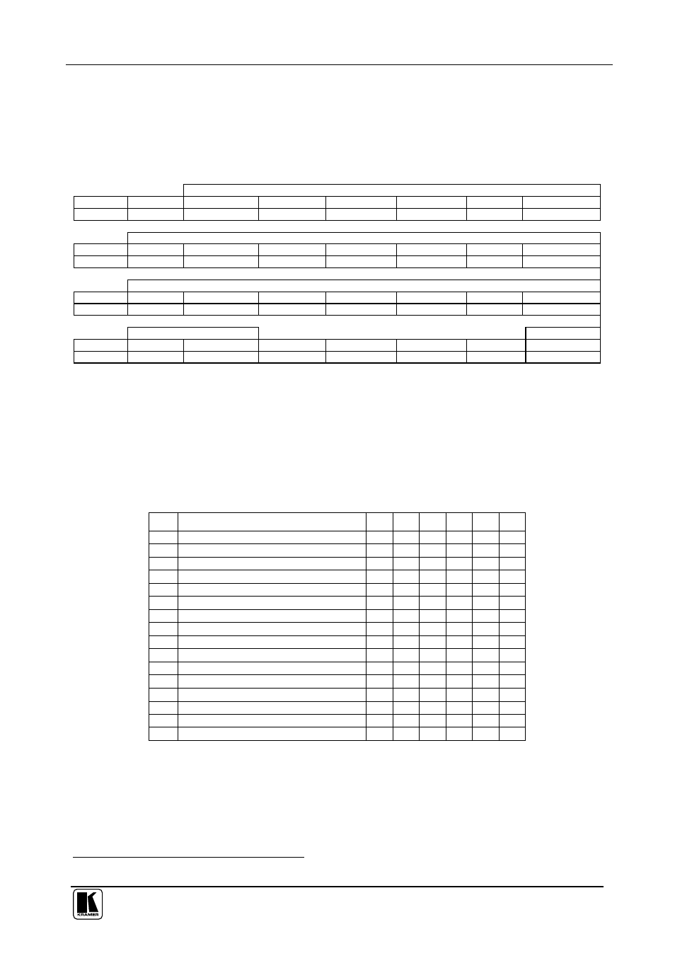
Table 4: Structure of the Protocol
MSB
LSB
INSTRUCTION
0
TO PC
I5
I4
I3
I2
I1
I0
7
6
5
4
3
2
1
0
1st byte
DATA
1
D6
D5
D4
D3
D2
D1
D0
7
6
5
4
3
2
1
0
2nd byte
EXTENDED DATA
1
E6
E5
E4
E3
E2
E1
E0
7
6
5
4
3
2
1
0
3rd byte
MSB’s
ADDR
1
E7
D7
1
0
1
1
0
7
6
5
4
3
2
1
0
4th byte
1
Note that the MSB’s of the DATA (D7) and the EXTENDED DATA (E7) are in the fourth byte.
Terminology:
TO PC is the “DESTINATION BIT”
I4..I0 is the “INSTRUCTION”
D7..D0 is the “DATA”
E7..E0 is the “EXTENDED DATA”
A0 is the “LSB of the MACHINE ADDRESS”
The destination bit, TO PC, is 0 when sending from the PC to the machine, or 1 when sending from the machine to the PC.
Table 5: Instruction Set for the FC-7501
#
INSTRUCTION
I5
I4
I3
I2
I1
I0
0
Reset
0
0
0
0
0
0
1
Read video standard
0
0
0
0
0
1
2
Write video standard
0
0
0
0
1
0
3
Read front-panel switch (video format)
0
0
0
0
1
1
4
Press front-panel switch (video format)
0
0
0
1
0
0
5
Read video field rate
0
0
0
1
0
1
6
Force video standard
0
0
0
1
1
0
10
Write EEPROM data – low address
0
0
1
0
1
0
11
Read EEPROM data – low address
0
0
1
0
1
1
12
Write I²C
0
0
1
1
0
0
13
Read I²C
0
0
1
1
0
1
16
Error
0
1
0
0
0
0
20
Write EEPROM data – high address
0
1
0
1
0
0
21
Read EEPROM data – high address
0
1
0
1
0
1
57
Enable “Power-down save”
1
1
1
0
0
1
61
Identify machine
1
1
1
1
0
1
1 Note that the MSB’s of the DATA (D7) and the EXTENDED DATA (E7) are in the fourth byte