Advanced chipset features – Elitegroup EZ-Buddie2 D21 I4-3 Manual User Manual
Page 37
33
Advanced Chipset Features
These items define critical timing parameters of the motherboard. You should
leave the items on this page at their default values unless you are very famil-
iar with the technical specifications of your system hardware. If you change
the values incorrectly, you may introduce fatal errors or recurring instability
into your system.
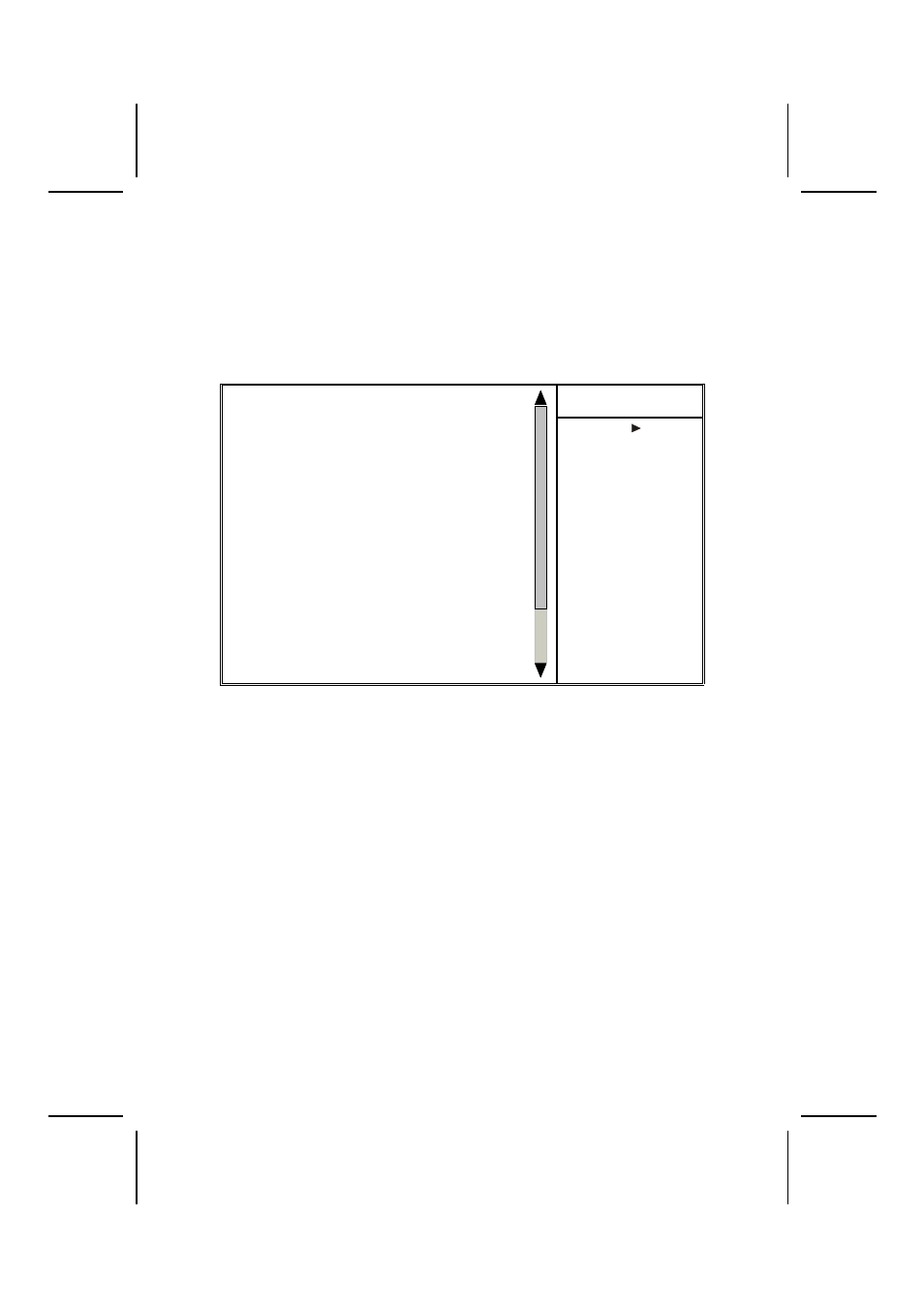
Phoenix – AwardBIOS CMOS Setup Utility
Advanced Chipset Features
Item Help
DRAM Timing Selectable
[By SPD
x CAS Latency Time
[2.5]
x Active to Precharge Delay
[7]
x DRAM RAS# to CAS# Delay
[3]
x DRAM RAS# Precharge
[3]
Memory Frequency For
[Auto]
System BIOS Cacheable
[Disabled]
Video BIOS Cacheable
[Disabled]
AGP Aperture Size (MB)
[128]
Init Display First
[PCI Slot]
** Photon Acceleration Technology **
Fast Chip Select
[Auto]
CPC
Addr/Control
[Auto]
Turbo
Mode
[Auto]
** On-chip VGA Setting **
On-Chip
VGA
[Enabled]
On-chip Frame Buffer Size
[8M]
Boot
Display
[Auto]
Menu Level
↑ ↓ → ← : Move
Enter : Select
+/-/PU/PD:Value:
F10: Save ESC: Exit F1:General Help
F5:Previous Values
F6:Fail-Safe Defaults
F7:Optimized Defaults
DRAM Timing Selectable (By SPD)
The value in this field depends on performance parameters of the installed
memory chips (DRAM). Do not change the value from the factory setting
unless you install new memory that has a different performance rating than
the original DRAMs.
CAS Latency Time: (2.5)
When synchronous DRAM is installed, the number of clock cycles of CAS
latency depends on the DRAM timing. Do not reset this field from the default
value specified by the system designer.
Active to Precharge Delay (7)
The precharge time is the number of cycles it takes for DRAM to accumulate
its charge before refresh.
DRAM RAS# to CAS# Delay (3)
This field lets you insert a timing delay between the CAS and RAS strobe sig-
nals, used when DRAM is written to, read from, or refreshed. Disabled gives
faster performance; and Enabled gives more stable performance.