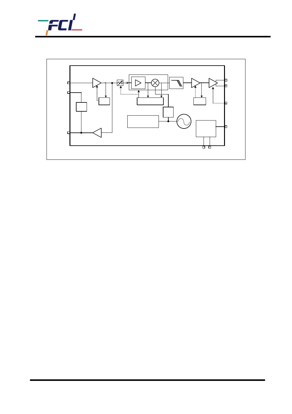
Fc5150, Block diagram, Tf (tracking filter) + mix (mixer) – Silicon Motion FC5150 User Manual
Page 4

FC5150
RF Silicon IC tuner
For Digital Cable TV standards
G
G
Preliminary
4 / 30
April. 2013
Future
Communications
Integrated circuit Inc.
Block diagram
AGC_BB
LNA
TF+MIX
CSF
PGA
VGA
ATTEN2
Passive
LT
AGC
AGC
AGC
I2C
RF_IN
LT_IN
LTO
SDATA SCLK
OUT_IP
OUT_IM
Fractional PLL
svG
ID
Figure 1. Block diagram
LNA
The first block of the receiver chain is a low-noise, highly linear amplifier (LNA). The FC5150 LNA
attenuation is controlled automatically and programmable via the I2C interface.
ATTEN2
The AGC drives a variable attenuator. This block provides 20 dB of total attenuation range in 0.25dB
steps.
TF (Tracking Filter) + MIX (Mixer)
The FC5150 has been designed to provide optimal image rejection. Using symmetry in the design of I
and Q paths of the receiver ensures that mismatch between the I and Q paths is minimized.
CSF
CSF (Channel Selection Filter) provides highly jammer rejection performance. And Bandwidth is
adjustable by register tuning, but it’s already optimized for system performance.
VGA
The VGA gain is controlled by the dc voltage applied to the AGC_BB pin. By varying the input dc
voltage from 0V to 3.3V (in case that VDD33 is 3.3V) the VGA total gain goes from minimum to
maximum. The gain control is linear in dB, with a typical slope around 15dB/V.
