Ac timing characteristics, Dc electrical characteristics (continued) – Rainbow Electronics MAX9921 User Manual
Page 3
MAX9921
Dual, 2-Wire Hall-Effect Sensor Interface
with Diagnostics
_______________________________________________________________________________________
3
Note 1: All DC specifications are 100% tested at T
A
= +25°C. AC specifications and specifications over -40°C to +125°C are guar-
anteed by design.
Note 2: C
L
is external load capacitance on the outputs for test only.
Note 3: These blanking times apply when the MAX9921 is operating in normal mode. Blanking times following power-up or startup
from shutdown mode are 20µs longer.
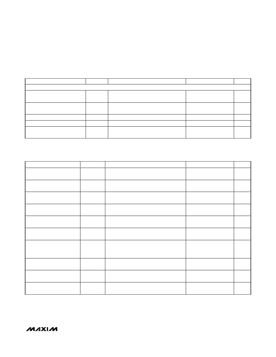
AC TIMING CHARACTERISTICS
(V
BAT
= 13.6V, V
DIAG
= 0V, V
OE
= 5V, IN1 = IN2 = no connection, R
ISET
= 63.4k
Ω, R
PU
= 10k
Ω at ERR, OUT1 and OUT2, T
A
= -40°C
to +125°C, unless otherwise noted. Typical values are at T
A
= +25°C.) (Notes 1 and 2)
DC ELECTRICAL CHARACTERISTICS (continued)
(V
BAT
= 13.6V, V
DIAG
= 0V, V
OE
= 5V, IN1 = IN2 = no connection, R
ISET
= 63.4k
Ω, R
PU
= 10k
Ω at ERR, OUT1 and OUT2, T
A
= -40°C
to +125°C, unless otherwise noted. Typical values are at T
A
= +25°C.) (Note 1)
PARAMETER
SYMBOL
CONDITIONS
MIN
TYP
MAX
UNITS
IN1, IN2 Blanking Time at Hall
Switch Power-Up
t
BL
I
IH
= -11.5mA to GND, time from V
IN_
=
500mV until OUT_ high, C
L
= 20pF (Note 3)
50
140
µs
IN1, IN2 Current Ramp Rate
After Turn-On
t
RAMP
V
IN
= GND
3.8
mA/µs
Delay from IN_ to OUT_ (Filter
Delay)
t
DEL
From I
IH
to I
IL
or from I
IL
to I
IH
, C
L
= 20pF,
Figure 1
6.5
µs
Delay from IN_ Fault to ERR
t
ERR
From I
IL
to I
SC
or from I
IH
to I
OC,
falling edge
only, C
L
= 20pF, Figure 1
31
ns
Delay from DIAG High to
OUT_ and ERR
t
DLH
Rising edge of DIAG to falling or rising edge
of outputs, C
L
= 20pF, Figure 1
350
ns
Delay from DIAG Low to OUT_
and ERR
t
DHL
Falling edge of DIAG to falling or rising edge
of outputs, C
L
= 20pF, Figure 1
1.6
µs
Delay Difference Between
Rising and Falling Edges for
Both Channels
t
DM
C
HALL-BYPASS
= 0.01µF, I
IH
= -11.5mA and
I
IL
= -7.2mA, C
L
= 20pF
20
ns
Delay Difference Between
Channels
t
CC
C
HALL-BYPASS
= 0.01µF, I
IH
= -11.5mA and
I
IL
= -7.2mA, C
L
= 20pF
100
ns
Maximum Frequency on Hall
Inputs
f
MAX
C
HALL-BYPASS
= 0.01µF, I
IH
= -11.5mA and
I
IL
= -7.2mA, C
L
= 20pF
50
kHz
IN_ Pulse Length Rejected by
Filter to OUT_
P
R
Figure 2
5.5
µs
PARAMETER
SYMBOL
CONDITIONS
MIN
TYP
MAX
UNITS
LOGIC I/O (OUT1, OUT2, ERR, DIAG, and OE)
Output Voltage Low (ERR, OUT1,
OUT2)
V
OL
Sink current = 1mA
0.4
V
Three-State Output Current (ERR,
OUT1, OUT2)
I
OZ
V
OE
= 0V, 0
≤ V
OUT_
≤ 5V
±1
µA
Input-Voltage High (DIAG, OE)
V
IH
2.1
V
Input-Voltage Low (DIAG, OE)
V
IL
0.8
V
Input Resistance to GND (DIAG,
OE)
R
IN
50
80
k
Ω