Pin configuration chip information – Rainbow Electronics MAX2130 User Manual
Page 7
Dynamic Linearity Adjustment
The LNA and loop-out amplifier linearity can be dynam-
ically adjusted by varying the amount of current
sourced by the BIAS port. The BIAS port is internally
biased to 1.2V. A resistor, R
BIAS
, connected from BIAS
to ground sets the bias current. An additional resistor,
R
ADJ
, placed from the BIAS port to an external voltage
source, such as a digital-to-analog converter (DAC),
varies the current sourced by the BIAS port. Choosing
R
ADJ
= R
BIAS
= 20k
Ω and varying the voltage of the
DAC from ground to 2.4V effectively varies the resis-
tance seen from the BIAS port from 10k
Ω to an open
circuit. See Typical Application Circuit.
The DAC output voltage, V
ADJ
, required to set an equiv-
alent resistance to ground, R
EQ
, seen by the BIAS port,
can be calculated with the following equation:
V
ADJ
= 2.4V - (R
BIAS
✕
V
BIAS
) / R
EQ
where R
ADJ
= R
BIAS
, V
BIAS
= 1.2V, R
EQ
≥ 10kΩ.
Power-Supply Bypassing
Proper voltage-supply bypassing is essential for high-
frequency circuit stability. Bypass the V
CC
pin with a
1000pF capacitor in parallel with a 47pF capacitor,
located as close to the V
CC
pin as possible. Refer to
the MAX2130 EV kit for additional information.
MAX2130
Broadband, Two-Output, Low-Noise
Amplifier for TV Tuner Applications
_______________________________________________________________________________________
7
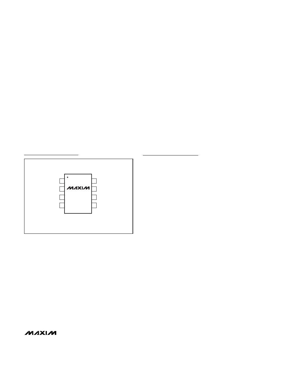
GND
OUT2
GND
1
2
8
7
OUT1
GND
IN
BIAS
V
CC
µMAX-EP
TOP VIEW
3
4
6
5
MAX2130
Pin Configuration
Chip Information
TRANSISTOR COUNT: 167