Pin description (continued) – Rainbow Electronics MAX1531 User Manual
Page 13
MAX1530/MAX1531
Multiple-Output Power-Supply Controllers for
LCD Monitors
______________________________________________________________________________________
13
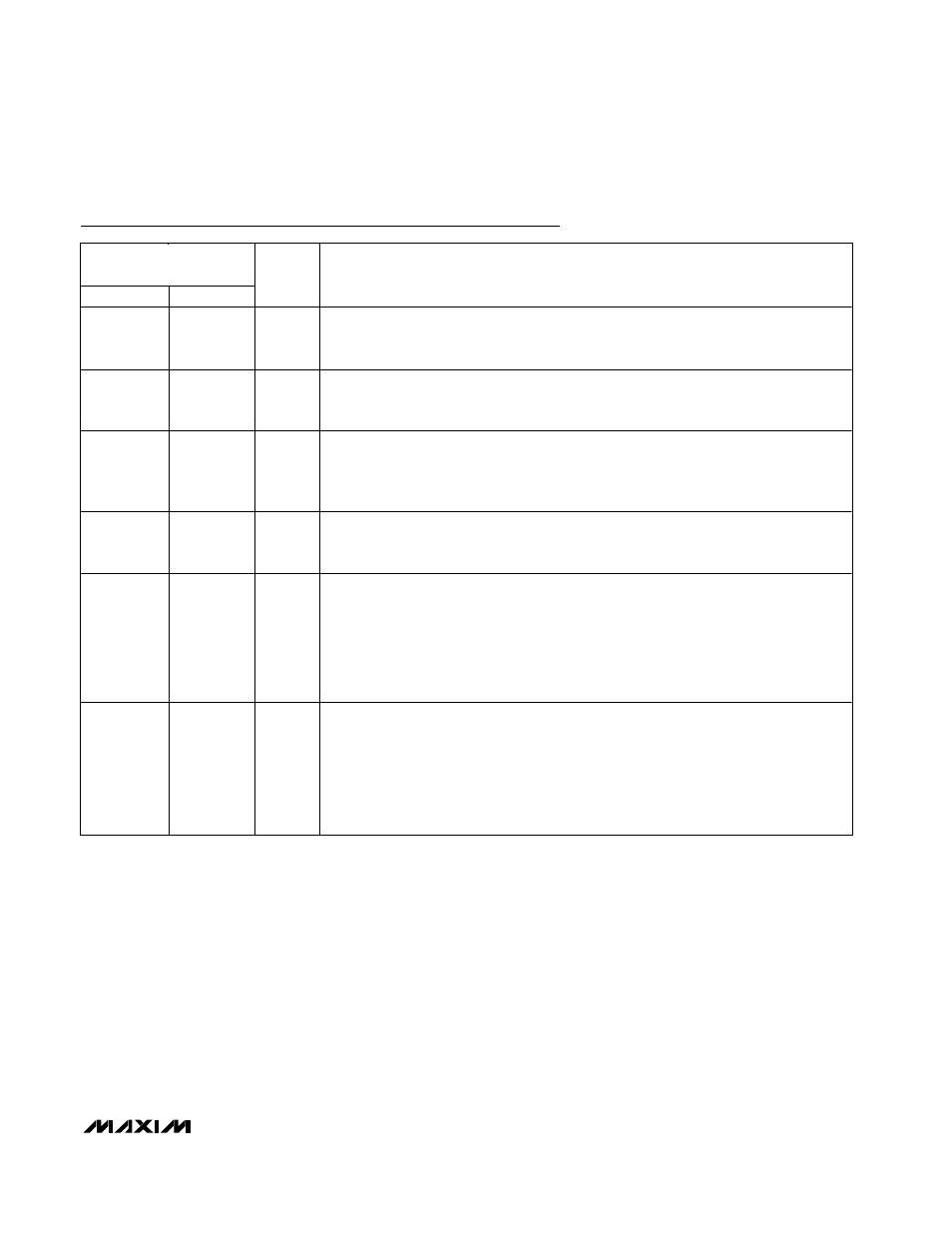
Pin Description (continued)
PIN
MAX1530
MAX1531
NAME
FUNCTION
—
7
FBL4
Source Drive Linear Regulator (LR4) Feedback Input. FBL4 regulates at 1.245V nominal.
Connect FBL4 to the center tap of a resistive voltage-divider between the LR4 output and
AGND to set the output voltage. Place the divider close to the FBL4 pin.
—
8
DRV4
Source Drive Linear Regulator (LR4) Base Drive. Open drain of an internal N-channel
MOSFET. Connect DRV4 to the base of an external PNP pass transistor to form a positive
linear regulator. (See the Pass Transistor Selection section.)
—
9
FBL5
Gate-Off Linear Regulator (LR5) Feedback Input. FBL5 regulates at 125mV nominal.
Connect FBL5 to the center tap of a resistive voltage-divider between the LR5 output and
the internal 5V linear regulator output (VL) to set the output voltage. Place the divider close
to the FBL5 pin.
—
10
DRV5
Gate-Off Linear Regulator (LR5) Base Drive. Open drain of an internal P-channel MOSFET.
Connect DRV5 to the base of an external NPN pass transistor to form a negative linear
voltage regulator. (See the Pass Transistor Selection section.)
—
18
ONL4
Source Drive Linear Regulator (LR4) Enable Input. When EN is above its enable threshold,
VL is above its UVLO threshold, and ONL4 is greater than the internal reference, LR4 is
enabled. Drive ONL4 with a logic signal or, for automatic sequencing, connect a capacitor
from ONL4 to AGND. If SEQ is high, EN is above its threshold, and VL is above its UVLO
threshold, an internal 2µA (typ) current source charges the capacitor. Otherwise, an
internal switch discharges the capacitor. Connecting various capacitors to each ONL_ pin
allows the programming of the startup sequence.
—
19
ONL5
Gate-Off Linear Regulator (LR5) Enable Input. When EN is above its enable threshold, VL
is above its UVLO threshold, and ONL5 is greater than the internal reference, LR5 is
enabled. Drive ONL5 with a logic signal or, for automatic sequencing, connect a capacitor
from ONL5 to AGND. If SEQ is high, EN is above its threshold, and VL is above its UVLO
threshold, an internal 2µA (typ) current source charges the capacitor. Otherwise, an
internal switch discharges the capacitor. Connecting various capacitors to each ONL_ pin
allows the programming of the startup sequence.