Typical operating characteristics (continued), Pin description – Rainbow Electronics MAX1531 User Manual
Page 10
MAX1530/MAX1531
Multiple-Output Power-Supply Controllers for
LCD Monitors
10
______________________________________________________________________________________
Typical Operating Characteristics (continued)
(Circuit of Figure 1; including R5, R6, and D2; T
A
= +25°C, unless otherwise noted.)
Pin Description
PIN
MAX1530
MAX1531
NAME
FUNCTION
1
1
DRV2
Gamma Linear Regulator (LR2) Base Drive. Open drain of an internal N-channel MOSFET.
Connect DRV2 to the base of an external PNP pass transistor to form a positive linear
regulator. (See the Pass Transistor Selection section.)
2
2
FBL2
Gamma Linear Regulator (LR2) Feedback Input. FBL2 regulates at 1.245V nominal.
Connect FBL2 to the center tap of a resistive voltage-divider between the LR2 output and
AGND to set the output voltage. Place the divider close to the FBL2 pin.
3
3
FBL3
Gate-On Linear Regulator (LR3) Feedback Input. FBL3 regulates at 1.245V nominal.
Connect FBL3 to the center tap of a resistive voltage-divider between the LR3 output and
AGND to set the output voltage. Place the divider close to the FBL3 pin.
4
4
DRV3
Gate-On Linear Regulator (LR3) Base Drive. Open drain of an internal N-channel MOSFET.
Connect DRV3 to the base of an external PNP pass transistor to form a positive linear
regulator. (See the Pass Transistor Selection section.)
5–10, 18, 19
—
N. C.
No Connection. Not internally connected.
11
11
RSTIN
Adjustable Reset Input. RESET asserts low when the monitored voltage is less than the
reset trip threshold. RESET goes to a high-impedance state only after the monitored
voltage remains above the reset trip threshold for the duration of the reset timeout period.
Connect RSTIN to the center tap of a resistive voltage-divider between the monitored
output voltage and AGND to set the reset trip threshold. The internal RSTIN threshold of
90% of 1.238V allows direct connection of RSTIN to any of the device’s positive feedback
pins.
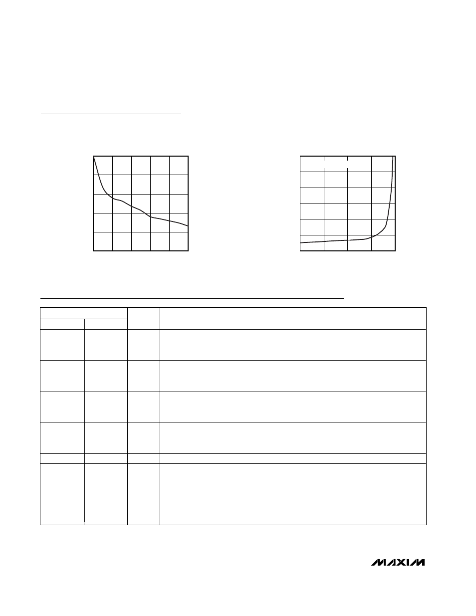
LR5 NORMALIZED LOAD REGULATION
MAX1530 toc25
LOAD CURRENT (mA)
VOLTAGE ERROR (%)
40
30
20
10
-0.8
-0.6
-0.4
-0.2
0
-1.0
0
50
LR5 NORMALIZED LINE REGULATION
MAX1530 toc26
INPUT VOLTAGE (V)
OUTPUT-VOLTAGE ERROR (%)
-13
-17
-21
0
0.2
0.4
0.6
0.8
1.0
-0.2
-25
-9
20mA LOAD CURRENT