Max1198, Grounding, bypassing, and board layout – Rainbow Electronics MAX1198 User Manual
Page 18
MAX1198
shifted with respect to the in-phase component. At the
receiver, the QAM signal is divided down into its I and
Q components, essentially representing the modulation
process reversed.
Figure 10 displays the demodulation
process performed in the analog domain, using the
dual matched 3.3V, 8-bit ADC MAX1198 and the
MAX2451 quadrature demodulator to recover and
digitize the I and Q baseband signals. Before being
digitized by the MAX1198, the mixed down-signal com-
ponents may be filtered by matched analog filters, such
as Nyquist or pulse-shaping filters, which remove
unwanted images from the mixing process, thereby
enhancing the overall signal-to-noise (SNR) perfor-
mance and minimizing intersymbol interference.
Grounding, Bypassing,
and Board Layout
The MAX1198 requires high-speed board layout design
techniques. Locate all bypass capacitors as close to
the device as possible, preferably on the same side as
the ADC, using surface-mount devices for minimum
inductance. Bypass V
DD
, REFP, REFN, and COM with
two parallel 0.1µF ceramic capacitors and a 2.2µF
bipolar capacitor to GND. Follow the same rules to
bypass the digital supply (OV
DD
) to OGND. Multilayer
boards with separated ground and power planes
produce the highest level of signal integrity. Consider
the use of a split ground plane arranged to match the
Dual, 8-Bit, 100Msps, 3.3V, Low-Power ADC
with Internal Reference and Parallel Outputs
18
______________________________________________________________________________________
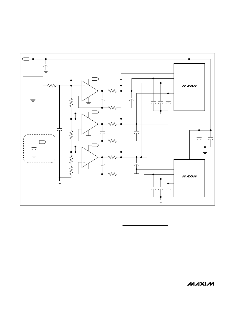
1/4 MAX4252
MAX6066
1/4 MAX4252
1/4 MAX4252
1.47k
Ω
21.5k
Ω
21.5k
Ω
21.5k
Ω
21.5k
Ω
21.5k
Ω
47
Ω
3.3V
3.3V
11
2
2
3
4
1
1
REFOUT
REFP
REFIN
1
µF
10
µF
6V
MAX1198
N = 1
REFN
29
N.C.
N.C.
31
32
1
2
29
31
32
1
2
COM
REFOUT
NOTE: ONE FRONT-END REFERENCE CIRCUIT DESIGN MAY BE USED WITH UP TO 32 ADCs.
REFP
REFIN
MAX1198
N = 32
REFN
COM
2.0V AT 8mA
3
0.1
µF
0.1
µF
MAX4254 POWER-SUPPLY
BYPASSING. PLACE CAPACITOR
AS CLOSE AS POSSIBLE TO
THE OP AMP.
3.3V
1.47k
Ω
47
Ω
3.3V
1.5V
11
6
5
4
7
10
µF
6V
1.5V AT 0mA
1.47k
Ω
47
Ω
3.3V
11
9
10
4
8
10
µF
6V
0.1
µF
0.1
µF
0.1
µF
0.1
µF
0.1
µF
2.2
µF
10V
0.1
µF
0.1
µF
1.0V AT -8mA
330
µF
6V
330
µF
6V
330
µF
6V
2.0V
1.0V
Figure 9. External Unbuffered Reference Drive with MAX4252 and MAX6066