Rainbow Electronics MAX1198 User Manual
Page 13
Match the impedance of INA+ and INA-, as well as
INB+ and INB-, and set the common-mode voltage to
mid supply (V
DD
/2) for optimum performance.
Analog Inputs and Reference
Configurations
The full-scale range of the MAX1198 is determined by
the internally generated voltage difference between
REFP (V
DD
/2 + V
REFIN
/4) and REFN (V
DD
/2 - V
REFIN
/4).
The full-scale range for both on-chip ADCs is
adjustable through the REFIN pin, which is provided for
this purpose.
The MAX1198 provides three modes of reference operation:
• Internal reference mode
• Buffered external reference mode
• Unbuffered external reference mode
In internal reference mode, connect the internal refer-
ence output REFOUT to REFIN through a resistor (e.g.,
10k
Ω) or resistor-divider, if an application requires a
reduced full-scale range. For stability and noise-filtering
purposes, bypass REFIN with a >10nF capacitor to
GND. In internal reference mode, REFOUT, COM,
REFP, and REFN become low-impedance outputs.
In buffered external reference mode, adjust the refer-
ence voltage levels externally by applying a stable and
accurate voltage at REFIN. In this mode, COM, REFP,
and REFN are outputs. REFOUT can be left open or
connected to REFIN through a >10k
Ω resistor.
In unbuffered external reference mode, connect REFIN
to GND. This deactivates the on-chip reference buffers
for REFP, COM, and REFN. With their buffers shut
down, these nodes become high-impedance inputs
and can be driven through separate, external reference
sources.
For detailed circuit suggestions and how to drive this
dual ADC in buffered/unbuffered external reference
mode, see the Applications Information section.
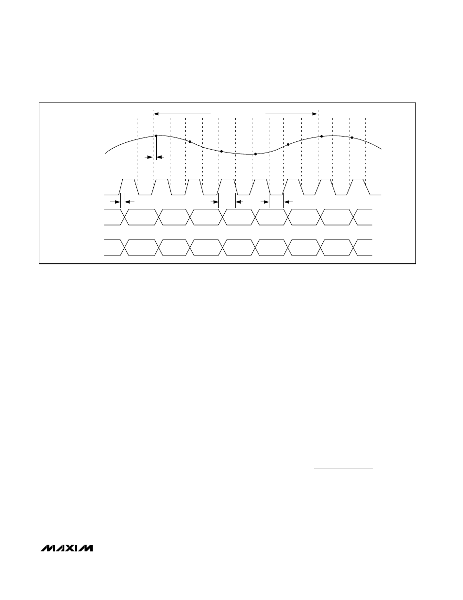
Clock Input (CLK)
The MAX1198’s CLK input accepts a CMOS-compati-
ble clock signal. Since the interstage conversion of the
device depends on the repeatability of the rising and
falling edges of the external clock, use a clock with low
jitter and fast rise and fall times (<2ns). In particular,
sampling occurs on the rising edge of the clock signal,
requiring this edge to provide lowest possible jitter. Any
significant aperture jitter would limit the SNR perfor-
mance of the on-chip ADCs as follows:
where f
IN
represents the analog input frequency and
t
AJ
is the time of the aperture jitter.
Clock jitter is especially critical for undersampling
applications. The clock input should always be consid-
ered as an analog input and routed away from any ana-
log input or other digital signal lines.
SNR
f
t
IN
AJ
log
=
Ч
Ч
Ч
Ч
20
1
2
π
MAX1198
Dual, 8-Bit, 100Msps, 3.3V, Low-Power ADC
with Internal Reference and Parallel Outputs
______________________________________________________________________________________
13
N - 6
N
N - 5
N + 1
N - 4
N + 2
N - 3
N + 3
N - 2
N + 4
N - 1
N + 5
N
N + 6
N + 1
5-CLOCK-CYCLE LATENCY
ANALOG INPUT
CLOCK INPUT
DATA OUTPUT
D7A–D0A
t
DO
t
CH
t
CL
N - 6
N - 5
N - 4
N - 3
N - 2
N - 1
N
N + 1
DATA OUTPUT
D7B–D0B
t
AD
Figure 3. System Timing Diagram