Max1198, Applications information – Rainbow Electronics MAX1198 User Manual
Page 14
MAX1198
The MAX1198 clock input operates with a voltage thresh-
old set to V
DD
/2. Clock inputs with a duty cycle other
than 50% must meet the specifications for high and low
periods as stated in the Electrical Characteristics table.
System Timing Requirements
Figure 3 depicts the relationship between the clock
input, analog input, and data output. The MAX1198
samples at the rising edge of the input clock. Output
data for channels A and B is valid on the next rising
edge of the input clock. The output data has an internal
latency of five clock cycles. Figure 3 also determines
the relationship between the input clock parameters
and the valid output data on channels A and B.
Digital Output Data (D0A/B–D7A/B), Output
Data Format Selection (T/B), Output
Enable (
OE
)
All digital outputs, D0A–D7A (channel A) and D0B–D7B
(channel B), are TTL/CMOS-logic compatible. There is a
five-clock-cycle latency between any particular sample
and its corresponding output data. The output
coding can either be straight offset binary or two’s com-
plement (Table 1) controlled by a single pin (T/B). Pull
T/B low to select offset binary and high to activate two’s
complement output coding. The capacitive load on the
digital outputs D0A–D7A and D0B–D7B should be kept
as low as possible (<15pF), to avoid large digital cur-
rents that could feed back into the analog portion of the
MAX1198, thereby degrading its dynamic performance.
Using buffers on the digital outputs of the ADCs can fur-
ther isolate the digital outputs from heavy capacitive
loads. To further improve the dynamic performance of
the MAX1198, small-series resistors (e.g., 100
Ω) may
be added to the digital output paths close to the
MAX1198.
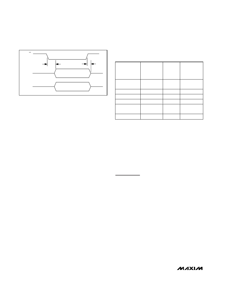
Figure 4 displays the timing relationship between out-
put enable and data output valid, as well as power-
down/wakeup and data output valid.
Power-Down and Sleep Modes
The MAX1198 offers two power-save modes—sleep
mode (SLEEP) and full power-down (PD) mode. In
sleep mode (SLEEP = 1), only the reference bias circuit
is active (both ADCs are disabled), and current con-
sumption is reduced to 3.2mA.
To enter full power-down mode, pull PD high. With OE
simultaneously low, all outputs are latched at the last
value prior to power-down. Pulling OE high forces the
digital outputs into a high-impedance state.
Applications Information
Figure 5 depicts a typical application circuit containing
two single-ended-to-differential converters. The internal
reference provides a V
DD
/2 output voltage for level-
shifting purposes. The input is buffered and then split
to a voltage follower and inverter. One lowpass filter per
amplifier suppresses some of the wideband noise
associated with high-speed op amps. The user can
select the R
ISO
and C
IN
values to optimize the filter per-
formance, to suit a particular application. For the appli-
cation in Figure 5, a R
ISO
of 50
Ω is placed before the
capacitive load to prevent ringing and oscillation. The
22pF C
IN
capacitor acts as a small filter capacitor.
Using Transformer Coupling
An RF transformer (Figure 6) provides an excellent
solution to convert a single-ended source signal to a
fully differential signal, required by the MAX1198 for
optimum performance. Connecting the center tap of the
transformer to COM provides a V
DD
/2 DC level shift to
the input. Although a 1:1 transformer is shown, a step-
up transformer can be selected to reduce the drive
Dual, 8-Bit, 100Msps, 3.3V, Low-Power ADC
with Internal Reference and Parallel Outputs
14
______________________________________________________________________________________
OUTPUT
D7A–D0A
OE
t
DISABLE
t
ENABLE
HIGH-Z
HIGH-Z
VALID DATA
OUTPUT
D7B–D0B
HIGH-Z
HIGH-Z
VALID DATA
Figure 4. Output Timing Diagram
ST RA IG HT
O F FSET
B INA R Y
T WO’S
C O M PL EM EN T
D IFF ER EN T IAL
IN PU T
VO LT A G E*
D IFF ER EN T IAL
IN PU T
T/B = 0
T/B = 1
V
REF
x 255/256
+Full Scale
- 1LSB
1111 1111
0111 1111
V
REF
x 1/256
+1LSB
1000 0001
0000 0001
0
Bipolar Zero
1000 0000
0000 0000
-V
REF
x 1/256
-1LSB
0111 1111
1111 1111
-V
REF
x 255/256
-Full Scale
+ 1LSB
0000 0001
1000 0001
-V
REF
x 256/256
-Full Scale
0000 0000
1000 0000
Table 1. MAX1198 Output Codes For
Differential Inputs
*V
REF
= V
REFP
- V
REFN