Detailed description, Pin description (continued) – Rainbow Electronics MAX1774 User Manual
Page 11
MAX1774
Dual, High-Efficiency, Step-Down
Converter with Backup Battery Switchover
_______________________________________________________________________________________
11
Detailed Description
The MAX1774 dual step-down DC-DC converter is
designed to power PDA, palmtop, and subnotebook
computers. Normally, these devices require two sepa-
rate power supplies–one for the processor and another
higher voltage supply for the peripheral circuitry. The
MAX1774 provides an adjustable +1.25V to +5.5V main
output designed to power the peripheral circuitry of
PDAs and similar devices. The main output delivers up
to 2A output current. The lower voltage core converter
has an adjustable +1.0V to +5.0V output, providing up
to 1.5A output current. Both regulators utilize a propri-
etary regulation scheme allowing PWM operation at
medium to heavy loads, and automatically switch to
pulse skipping at light loads for improved efficiency.
Under low-battery conditions, the MAX1774 enters
backup mode, making use of a low-voltage backup
battery and a step-up regulator to power the output.
Figure 1 is the MAX1774 typical application circuit.
Operating Modes for the
Step-Down Converters
When delivering low output currents, the MAX1774 oper-
ates in discontinuous conduction mode. Current through
the inductor starts at zero, rises as high as the minimum
current limit (I
MIN
), then ramps down to zero during
PIN
QSOP
QFN
NAME
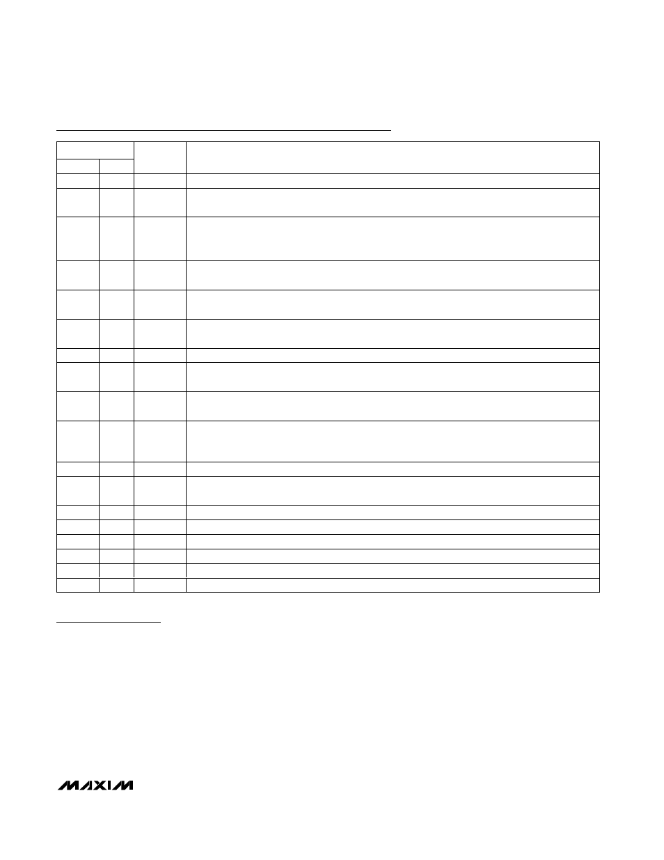
FUNCTION
—
10
LXB2
Backup Converter Switching Node. Connect LXB2 to LXB as close to the IC as possible.
13
11
BIN
Backup Batter y Inp ut. C onnect BIN to the outp ut of the b ackup b oost r eg ul ator . Byp ass BIN w i th a 10µF or
g r eater cap aci tor to GN D . W hen the M AX 1774 i s i n b ackup m od e, BIN p ow er s the m ai n outp ut.
14
12
BKOFF
Backup D i sab l e Inp ut. D r i vi ng BKO FF b el ow + 0.5V d i sab l es the b ackup m od e. In b ackup m od e, the
d evi ce enter s shutd ow n w hen thi s p i n i s p ul l ed l ow . BKO FF can b e d r i ven fr om a d i g i tal si g nal or can b e
used as a l ow b atter y d etector to d i sab l e the b ackup conver ter w hen the b ackup b atter y i s l ow .
15
13
ACI
AC Adapter Low-Voltage Detect Input. Connect to adapter DC input. When the voltage at ACI falls
below the voltage at INS plus +0.22V, ACO asserts.
16
14
DBI
D ead Batter y Inp ut. C onnect D BI to the m ai n b atter y thr oug h a r esi sti ve voltage-divider. W hen D BI d r op s
b el ow + 1.20V , no AC ad ap ter i s connected ( ACO i s l ow , b ut m ai n outp ut sti l l avai l ab l e) , BKU P asser ts.
17
15
LBI
Low-Battery Input. Connect LBI to the main battery through a r esi sti ve voltage-divider. When the
voltage at LBI drops below +1.20V, LBO asserts.
18
16
REF
Reference Voltage Output. Bypass REF to GND with a 0.22µF or greater capacitor.
—
17, 25,
29
N.C.
No Connection. Not Internally Connected.
19
18
FBM
Main Output Feedback. Connect FBM to a resistive voltage-divider to set main output voltage
between +1.25V to +5.5V.
20
19
CS+
Main Regulator High-Side Current-Sense Input. Connect the sense resistor between CS+ and CS-.
This voltage is used to set the current limit and to turn off the synchronous rectifier when the
inductor current approaches zero.
21
20
CS-
Main Regulator Low-Side Current-Sense Input. Connect CS- to the main output.
22
21
FBC
C or e Outp ut Feed b ack. C onnect FBC to a resistive voltage-divider to set cor e outp ut b etw een + 1.0V
to + 5.0V .
23
22
GND
Analog Ground
24
23
INC
Core Supply Input
25
24
ACO
Low AC Output. Open drain ACO asserts when ACI falls below the main output voltage plus 0.22V.
26
26
LBO
Open-Drain Low-Battery Output. LBO asserts when LBI falls below +1.20V.
27
27
INS
Power-Supply Input Voltage Sense Input. Connect INS to the power-supply input voltage.
28
28
LXC
Core Converter Switching Node
Pin Description (continued)