Detailed description, Digital interface – Rainbow Electronics MAX118 User Manual
Page 7
MAX114/MAX118
+5V, 1Msps, 4 & 8-Channel,
8-Bit ADCs with 1µA Power-Down
_______________________________________________________________________________________
7
_______________Detailed Description
Converter Operation
The MAX114/MAX118 use a half-flash conversion tech-
nique (see
Functional Diagram) in which two 4-bit flash
ADC sections achieve an 8-bit result. Using 15 com-
parators, the flash ADC compares the unknown input
voltage to the reference ladder and provides the upper
four data bits. An internal digital-to-analog converter
(DAC) uses the four most significant bits (MSBs) to
generate both the analog result from the first flash con-
version and a residue voltage that is the difference
between the unknown input and the DAC voltage. The
residue is then compared again with the flash com-
parators to obtain the lower four data bits (LSBs).
An internal analog multiplexer enables the devices to
read four (MAX114) or eight (MAX118) different analog
voltages under microprocessor (µP) control. One of the
MAX118’s analog channels, IN8, is internally hard-
wired and always reads V
REF+
when selected.
Power-Down Mode
In burst-mode or low sample-rate applications, the
MAX114/MAX118 can be shut down between conver-
sions, reducing supply current to microamp levels (see
Typical Operating Characteristics). A logic low on the
PWRDN pin shuts the devices down, reducing supply
current typically to 1µA when powered from a single +5V
supply. A logic high on
PWRDN wakes up the
MAX114/MAX118, and the selected analog input enters
the track mode. The signal is fully acquired after 360ns
(this includes both the power-up delay and the track/hold
acquisition time), and a new conversion can be started.
If the power-down feature is not required, connect
PWRDN to V
DD
. For minimum current consumption, keep
digital inputs at the supply rails in power-down mode.
Refer to the
Reference section for information on reduc-
ing reference current during power-down.
___________________Digital Interface
The MAX114/MAX118 have two basic interface modes,
which are set by the MODE pin. When MODE is low,
the converters are in read mode; when MODE is high,
the converters are set up for write-read mode. The A0,
A1, and A2 inputs control channel selection, as shown
in Table 1. The address must be valid for a minimum
time, t
ACQ
, before the next conversion starts.
Read Mode (MODE = 0)
In read mode, conversions and data access are con-
trolled by the
RD input (Figure 3). The comparator
inputs track the analog input voltage for the duration of
t
ACQ
. Initiate a conversion by driving
CS and RD low.
With µPs that can be forced into a wait state, hold
RD
low until output data appears. The µP starts the conver-
sion, waits, and then reads data with a single read
instruction.
DATA
OUTPUTS
DATA
OUTPUTS
C
L
R
L
= 3k
C
L
a) HIGH-Z TO VOH
b) HIGH-Z TO VOL
R
L
= 3k
V
DD
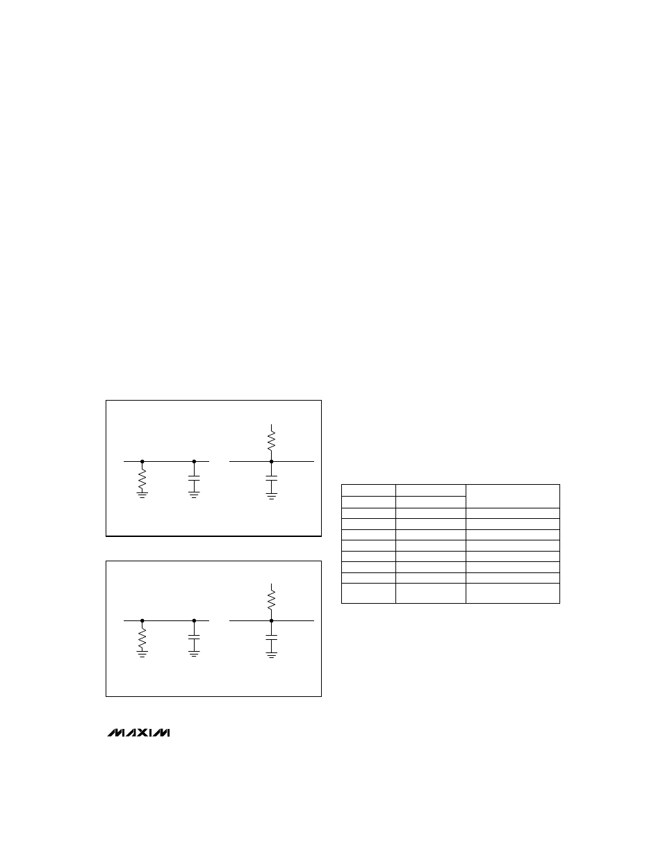
Figure 1. Load Circuits for Data-Access Time Test
DATA
OUTPUTS
10pF
3k
10pF
a) VOH TO HIGH-Z
b) VOL TO HIGH-Z
3k
V
DD
DATA
OUTPUTS
Figure 2. Load Circuits for Data-Hold Time Test
IN2
IN1
0
1
SELECTED CHANNEL
IN4
IN3
1
1
1
0
IN6
IN5
—
—
IN8
(reads V
REF+
if selected)
IN7
—
—
—
—
—
—
MAX114
0
0
Table 1. Truth Table for Input Channel
Selection
0
0
1
0
1
1
0
1
0
1
0
1
1
1
1
1
1
0
1
0
0
MAX118
0
0
0
A2
A1
A0
A1
A0