Rainbow Electronics MAX118 User Manual
Page 10

MAX114/MAX118
to break this current path during power-down. The FET
should have an on-resistance of less than 2
Ω
with a 5V
gate drive. When REF- is switched, as in Figure 7d, a
new conversion can be initiated after waiting a period
of time equal to the power-up delay (t
UP
) plus the N-
channel FET’s turn-on time.
Although REF+ is frequently connected to V
DD
, the cir-
cuit of Figure 7d uses a low-current, low-dropout,
4.096V voltage reference: the MAX874. Since the
MAX874 cannot continuously furnish enough current for
the reference resistance, this circuit is intended for
applications where the MAX114/MAX118 are normally
in standby and are turned on in order to make mea-
surements at intervals greater than 65µs. C1 (the
capacitor connected to REF+) is slowly charged by the
MAX874 during the standby period, and furnishes the
reference current during the short measurement period.
C1’s 3.3µF value ensures a voltage drop of less than
1/2LSB when performing four to eight successive con-
versions. Larger capacitors reduce the error still further.
Use ceramic or tantalum capacitors for C1.
Initial Power-Up
When power is first applied, perform a conversion to ini-
tialize the MAX114/MAX118. Disregard the output data.
Bypassing
Use a 4.7µF electrolytic in parallel with a 0.1µF ceramic
capacitor to bypass V
DD
to GND. Minimize capacitor
lead lengths.
Bypass the reference inputs with 0.1µF capacitors, as
shown in Figures 7a, 7b, and 7c.
Analog Inputs
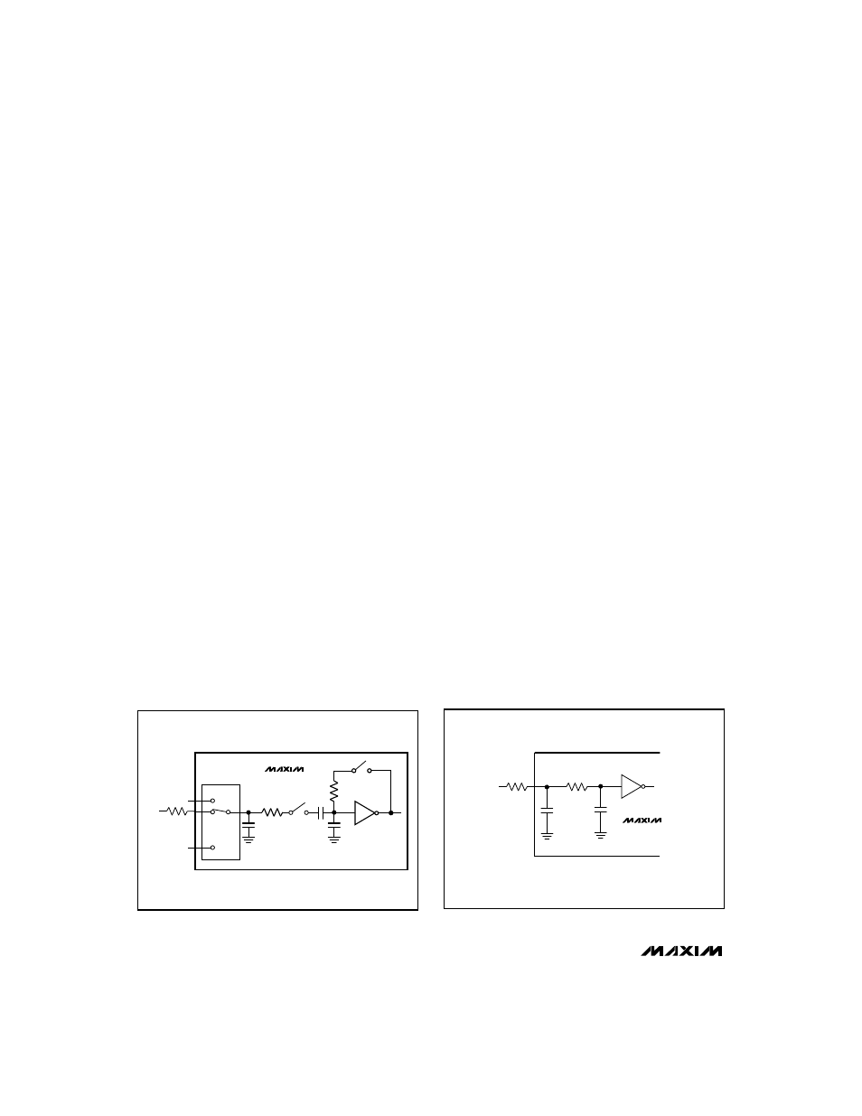
Figure 8 shows the equivalent circuit of the MAX114/
MAX118 input. When a conversion starts and
WR is
low, V
IN_
is connected to sixteen 0.6pF capacitors.
During this acquisition phase, the input capacitors
charge to the input voltage through the resistance of
the internal analog switches. In addition, about 22pF of
stray capacitance must be charged. The input can be
modeled as an equivalent RC network (Figure 9). As
source impedance increases, the capacitors take
longer to charge.
The typical 32pF input capacitance allows source resis-
tance as high as 800
Ω
without setup problems. For
larger resistances, the acquisition time (t
ACQ
) must be
increased.
Internal protection diodes, which clamp the analog
input to V
DD
and GND, allow the channel input pins to
swing from GND - 0.3V to V
DD
+ 0.3V without damage.
However, for accurate conversions near full scale, the
inputs must not exceed V
DD
by more than 50mV or be
lower than GND by 50mV.
If the analog input exceeds 50mV beyond the sup-
plies, limit the input current to no more than 2mA,
as excessive current will degrade the conversion
accuracy of the on channel.
Track/Hold
The track/hold enters hold mode when a conversion
starts (
RD low or WR low). INT goes low at the end of
the conversion, at which point the track/hold enters
track mode. The next conversion can start after the min-
imum acquisition time, t
ACQ
.
+5V, 1Msps, 4 & 8-Channel,
8-Bit ADCs with 1µA Power-Down
10
______________________________________________________________________________________
2k
R
IN
V
IN_
22pF
V
IN
MAX114
MAX118
10pF
Figure 9. RC Network Equivalent Input Model
R
ON
R
IN
V
IN2
MAX114
MAX118
.
.
.
T/H
MUX
Figure 8. Equivalent Input Circuit
