Rainbow Electronics MAX118 User Manual
Page 2
MAX114/MAX118
+5V, 1Msps, 4 & 8-Channel,
8-Bit ADCs with 1µA Power-Down
2
_______________________________________________________________________________________
ABSOLUTE MAXIMUM RATINGS
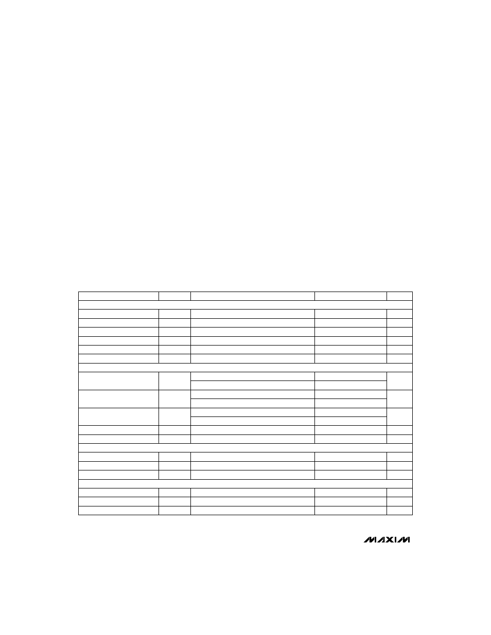
ELECTRICAL CHARACTERISTICS
(V
DD
= +5V ±5%, REF+ = 5V, REF- = GND, Read Mode (MODE = GND), T
A
= T
MIN
to T
MAX
, unless otherwise noted.)
Stresses beyond those listed under “Absolute Maximum Ratings” may cause permanent damage to the device. These are stress ratings only, and functional
operation of the device at these or any other conditions beyond those indicated in the operational sections of the specifications is not implied. Exposure to
absolute maximum rating conditions for extended periods may affect device reliability.
V
DD
to GND ..............................................................-0.3V to +7V
Digital Input Voltage to GND ......................-0.3V to (V
DD
+ 0.3V)
Digital Output Voltage to GND ...................-0.3V to (V
DD
+ 0.3V)
REF+ to GND..............................................-0.3V to (V
DD
+ 0.3V)
REF- to GND...............................................-0.3V to (V
DD
+ 0.3V)
IN_ to GND .................................................-0.3V to (V
DD
+ 0.3V)
Continuous Power Dissipation (T
A
= +70°C)
24-Pin Narrow Plastic DIP
(derate 13.33mW/°C above +70°C)....................................1.08W
24-Pin SSOP (derate 8.00mW/°C above +70°C)..............640mW
24-Pin Narrow CERDIP
(derate 12.50mW/°C above +70°C) .........................................1W
28-Pin Wide Plastic DIP
(derate 14.29mW/°C above +70°C)....................................1.14W
28-Pin SSOP (derate 9.52mW/°C above +70°C)..............762mW
28-Pin Wide CERDIP
(derate 16.67mW/°C above +70°C)....................................1.33W
Operating Temperature Ranges
MAX114/MAX118C_ _...........................................0°C to +70°C
MAX114/MAX118E_ _ ........................................-40°C to +85°C
MAX114/MAX118M_ _ .....................................-55°C to +125°C
Storage Temperature Range .............................-65°C to +150°C
Lead Temperature (soldering, 10sec) .............................+300°C
V
IN
_
= 5Vp-p
MAX11_M, f
SAMPLE
= 740kHz, f
IN
_
= 195.7kHz
GND < V
IN
_
< V
DD
MAX11_C/E, f
SAMPLE
= 1MHz, f
IN
_
= 195.8kHz
No-missing-codes guaranteed
CONDITIONS
V
V
REF-
V
DD
REF+ Input Voltage Range
k
Ω
1
2
4
R
REF
Reference Resistance
pF
32
C
IN
_
Input Capacitance
µA
±3
I
IN
_
Input Leakage Current
V
V
REF-
V
REF+
V
IN
_
Input Voltage Range
V/µs
3.1
15
Input Slew Rate, Tracking
LSB
±1
TUE
Total Unadjusted Error
Bits
8
N
Resolution
MHz
1
Input Full-Power Bandwidth
dB
45
SINAD
Signal-to-Noise Plus
Distortion Ratio
45
LSB
±1
DNL
Differential Nonlinearity
LSB
±1
Zero-Code Error
LSB
±1
Full-Scale Error
LSB
±1/4
Channel-to-Channel Mismatch
UNITS
MIN
TYP
MAX
SYMBOL
PARAMETER
MAX11_M, f
SAMPLE
= 740kHz, f
IN
_
= 195.7kHz
MAX11_C/E, f
SAMPLE
= 1MHz, f
IN
_
= 195.8kHz
dB
-50
THD
Total Harmonic Distortion
-50
MAX11_M, f
SAMPLE
= 740kHz, f
IN
_
= 195.7kHz
MAX11_C/E, f
SAMPLE
= 1MHz, f
IN
_
= 195.8kHz
dB
50
SFDR
Spurious-Free Dynamic
Range
50
V
GND
V
REF+
REF- Input Voltage Range
ACCURACY
(Note 1)
DYNAMIC PERFORMANCE
ANALOG INPUT
REFERENCE INPUT