Rainbow Electronics MAX545 User Manual
Page 2
MAX544/MAX545
+5V, Serial-Input, Voltage-Output, 14-Bit DACs
2
_______________________________________________________________________________________
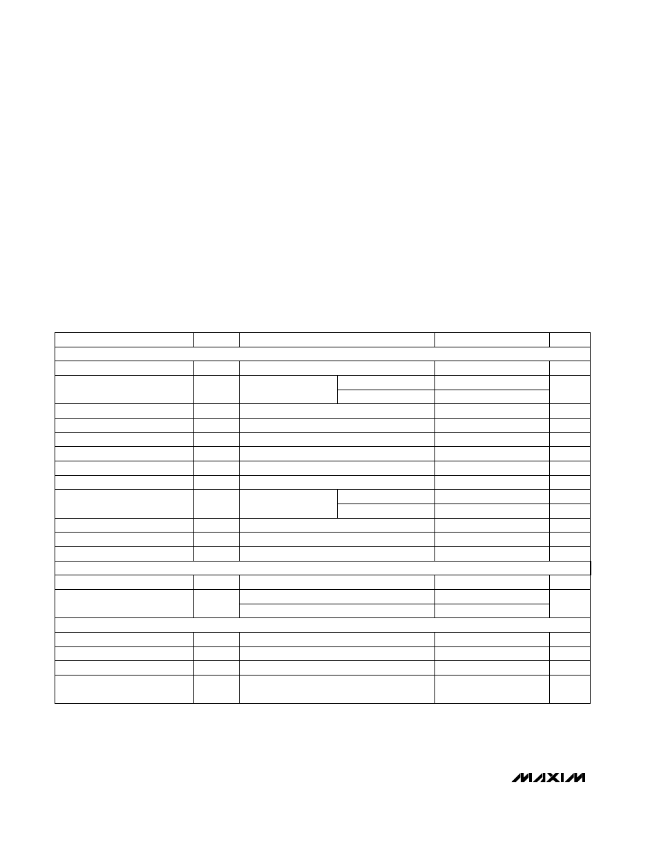
ABSOLUTE MAXIMUM RATINGS
ELECTRICAL CHARACTERISTICS
(V
DD
= +5V ± 5%, V
REF
= +2.5V, AGND = DGND = 0, T
A
= T
MIN
to T
MAX
, unless otherwise noted.)
Stresses beyond those listed under “Absolute Maximum Ratings” may cause permanent damage to the device. These are stress ratings only, and functional
operation of the device at these or any other conditions beyond those indicated in the operational sections of the specifications is not implied. Exposure to
absolute maximum rating conditions for extended periods may affect device reliability.
V
DD
to DGND ...........................................................-0.3V to +6V
CS, SCLK, DIN, LDAC to DGND ..............................-0.3V to +6V
REF, REFF, REFS to AGND ........................-0.3V to (V
DD
+ 0.3V)
AGND, AGNDF, AGNDS to DGND .......................-0.3V to +0.3V
OUT, INV to AGND DGND .......................................-0.3V to V
DD
RFB to AGND DGND...................................................-6V to +6V
Maximum Current into Any Pin............................................50mA
Continuous Power Dissipation (T
A
= +70°C)
8-Pin Plastic DIP (derate 9.09mW/°C above +70°C) .....727mW
8-Pin SO (derate 5.88mW/°C above +70°C) .................471mW
14-Pin Plastic DIP (derate 10.00mW/°C above +70°C) ...800mW
14-Pin SO (derate 8.33mW/°C above +70°C) ...............667mW
14-Pin Ceramic SB (derate 10.00mW/°C above +70°C...800mW
Operating Temperature Ranges
MAX544 _C_ A/MAX545_C_D ..............................0°C to +70°C
MAX544 _E_ A/MAX545_E_D............................-40°C to +85°C
MAX545BMJD .................................................-55°C to +125°C
Storage Temperature Range .............................-65°C to +150°C
Lead Temperature (soldering, 10s) .................................+300°C
MAX545, bipolar mode
Unipolar mode
(Note 3)
4.75V
≤ V
DD
≤ 5.25V
MAX545
Ratio error
V
DD
= 5V
R
FB
/R
INV
(Note 2)
CONDITIONS
k
Ω
9.0
R
REF
Reference Input Resistance
(Note 4)
11.5
V
2.0
3.0
V
REF
Reference Input Range
PSR
Power-Supply Rejection
LSB
±1.0
ppm/°C
±0.5
BZS
TC
Bipolar Zero Tempco
±10
±0.03
Bipolar Resistor Matching
1.0
R
OUT
DAC Output Resistance
k
Ω
6.25
±0.15
±0.5
Bits
14
N
Resolution
ppm/°C
±0.1
Gain-Error Tempco
LSB
Gain Error (Note 1)
±5
ppm/°C
±0.05
ZS
TC
Zero-Code Tempco
LSB
INL
Integral Nonlinearity
±0.6
Zero-Code Offset Error
UNITS
MIN
TYP
MAX
SYMBOL
PARAMETER
ZSE
mV
MAX54_A
Bipolar Zero Offset Error
C
L
= 10pF (Note 5)
25
V/µs
SR
Voltage-Output Slew Rate
DYNAMIC PERFORMANCE—ANALOG SECTION (R
L
=
∞, unipolar mode)
To ±
1
/
2
LSB of FS, C
L
= 10pF
1
µs
Output Settling Time
Major-carry transition
10
nVs
DAC Glitch Impulse
Code = 0000 hex; CS = V
DD
; LDAC = 0V;
SCLK, DIN = 0V to V
DD
levels
10
nVs
Digital Feedthrough
Guaranteed monotonic
LSB
±0.15
±0.9
DNL
Differential Nonlinearity
STATIC PERFORMANCE—ANALOG SECTION (R
L
=
∞)
REFERENCE INPUT
MAX545
MAX54_B
±0.15
±1
LSB
%
MAX545