Ac electrical characteristics (continued) – Rainbow Electronics MAX2701 User Manual
Page 7
MAX2700/MAX2701
1.8GHz to 2.5GHz Direct Downconversion
Receivers
_______________________________________________________________________________________
7
Note 1:
This is the recommended operating frequency range. The parts have been characterized over the specified frequency
range. Operation outside this range is possible but not guaranteed.
Note 2:
Guaranteed by design and characterization.
Note 3:
LNA is matched at input and output to 50
Ω
; f
1
= 1960MHz, f
2
= 1965MHz for MAX2700; f
1
= 2400MHz, f
2
= 2405MHz for
MAX2701; P
IN
= -30dBm per tone.
Note 4:
Mixer IIP3 test. For MAX2700, RFIN is matched to 50
Ω
at 1960MHz. At RFIN, apply f
1
= 1964.2MHz, f
2
= 1968.2MHz, P
IN
=
-25dBm per tone, and measure IM3 product power level at 200kHz. For MAX2701, RFIN is matched to 50
Ω
at 2400MHz. At
RFIN, apply f
1
= 2404.2MHz, f
2
= 2408.2MHz, P
IN
= -25dBm per tone, and measure IM3 product power level at 200kHz.
Note 5:
Mixer IIP2 test. For MAX2700, RFIN is matched to 50
Ω
at 1960MHz. At RFIN, apply f
1
= 1964.2MHz, f
2
= 1968.2MHz, P
IN
=
-25dBm per tone, and measure IM2 product power level at 4MHz. For MAX2701, RFIN is matched to 50
Ω
at 2400MHz. At
RFIN, apply f
1
= 2404.2MHz, f
2
= 2408.2MHz, P
IN
= -25dBm per tone, and measure IM2 product power level at 4MHz.
Note 6:
Mixer spurious attenuation response. Mixer is matched to 50
Ω
at 1800MHz and F
LO
= 900MHz (LO doubler enabled).
F
RFIN
= 1801MHz, P
RFIN
= -85dBm, F
SPUR
= 3601.5MHz, P
SPUR
= -60dBm. Measure IF at 1MHz and spurious at 1.5MHz at
the output. For better than 38dBc spurious attenuation response, output spurious level should be at least 10dB lower than
the IF signal level. In the (2 x LO) - (1 x RF) spurious product notation, LO denotes the frequency of the final LO driving the
I/Q mixers inputs.
Note 7:
Mixer gain specifications are production tested over LO power range.
Note 8:
A filter output impedance of 1.1k
Ω
can directly drive the VGA inputs since there is minimal mismatch loss between source and
VGA input impedance.
Note 9:
Electrolytic bypass cap to V
CC
not connected.
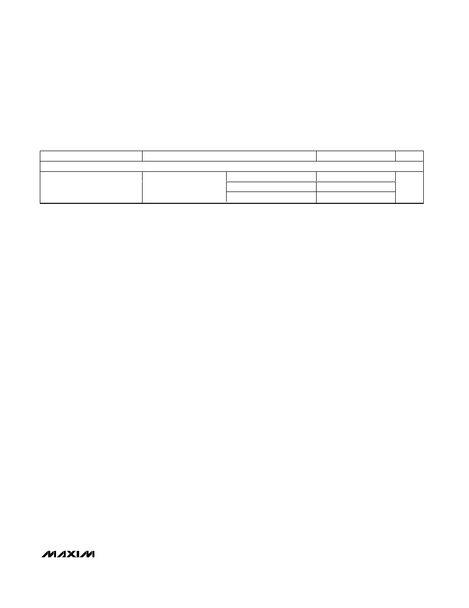
AC ELECTRICAL CHARACTERISTICS (continued)
(MAX2700/MAX2701 EV kit (Figure 3), V
CC
= +3.0V, T
A
= +25°C, SHDN = GAIN_SET = V
CC
, X2_EN = GND, CEXT+ connected to
CEXT-, P
LO
= -13dBm, F
LO
= 980MHz (MAX2700) and 1200MHz (MAX2701), P
LNAIN
= -30dBm, P
RFIN
= -25dBm, LNAIN and RFIN
(single-ended input to balun) driven from 50
Ω
source, LNAOUT terminated into load; MIX_I, MIX_Q AC-coupled to 2k
Ω
load; IIN1+,
QIN1+, IIN2+, QIN2+ driven from 1.1k
Ω
AC-coupled source; IOUT1, QOUT1 AC-coupled to 2k
Ω
; IOUT2, QOUT2 AC-coupled to
100
Ω
; input to VGAs, 20mVp-p at 1MHz tone, set V
AGC
= 1.25V, unless otherwise noted.)
PARAMETERS
CONDITIONS
MIN
TYP
MAX
UNITS
POWER SUPPLY
Mixer
57
VGA1
35
Power-Supply Ripple Rejection
V
C C
= 3.0V + 100m V
P P
fr eq uency = 100 to 300kH z,
V
OU T
= 0.3Vp - p ,
( N ote 9)
VGA2
28
dBc