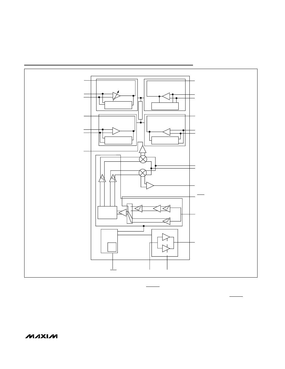
Functional diagram – Rainbow Electronics MAX2701 User Manual
Page 19
MAX2700/MAX2701
1.8GHz to 2.5GHz Direct Downconversion
Receivers
______________________________________________________________________________________
19
very low output impedance (<2
Ω
). The smallest load
that should be used is 600
Ω
. At the output of the I/Q
mixers’ buffers, baseband lowpass filters should be
used to provide adjacent and alternate channel selectiv-
ity. This reduces the level of adjacent channel and
close-in interferers to the input of the following base-
band amplifier.
The LO signal is applied externally to the LO input port.
An LO doubler circuit doubles the LO signal frequency
before it is applied to the mixer LO port. Connect
X2_EN to ground to enable the LO doubler circuit. With
this circuit enabled, the required LO frequency is half
that of the RF carrier frequency. Connect X2_EN to V
CC
to disable the frequency doubler circuit and the LO fre-
quency is the same as the RF carrier frequency. The
half LO frequency scheme results in the use of lower
frequency and lower cost VCOs. It also reduces the LO
leakage to the receiver’s input. The mixer is guaranteed
QOUT2
IOUT2
IIN2-
IIN2+
IOUT1
IIN1-
IIN1+
MIX_I
SHDN
LNAIN
BIAS
X2
BIAS
HIGH-GAIN AMP
GAIN_SET
QIN2-
QIN2+
QOUT1
QIN1-
QIN1+
RFIN+
MIX_Q
X2_EN
LO
LD GENERATOR
DOUBLER
BIAS
BLOCK
MST
SHDN
LNAOUT
RFIN-
MULTIPLEXER
AMP
AMP
I_CHANNEL
AGC1 I_CHANNEL
AGC1 Q_CHANNEL
AGC2 I_CHANNEL
AGC2 Q_CHANNEL
Q_CHANNEL
Q_CHANNEL
I_CHANNEL
DOUBLE BALANCED
MIXER
OFFSET CORRECTION
LOOP
OFFSET CORRECTION
LOOP
OFFSET CORRECTION
LOOP
OFFSET CORRECTION
LOOP
VGA CONTROL
POLYPHASE RC
QUADRATURE
GENERATOR
LOW-GAIN AMP
LNA BLOCK
Functional Diagram