Logic electrical characteristics, Lm77 – Rainbow Electronics LM77 User Manual
Page 6
Logic Electrical Characteristics
(Continued)
SERIAL BUS DIGITAL SWITCHING CHARACTERISTICS Unless otherwise noted, these specifications apply for +V
S
=+5 Vdc
±
10% for LM77CIM-5 and LM77CIMM-5, +V
S
=+3.3 Vdc
±
10% for LM77CIM-3 and LM77CIMM-3, CL (load capacitance) on
output lines = 80 pF unless otherwise specified. Boldface limits apply for T
A
= T
J
= T
MIN
to T
MAX
; all other limits T
A
= T
J
=
+25˚C, unless otherwise noted.
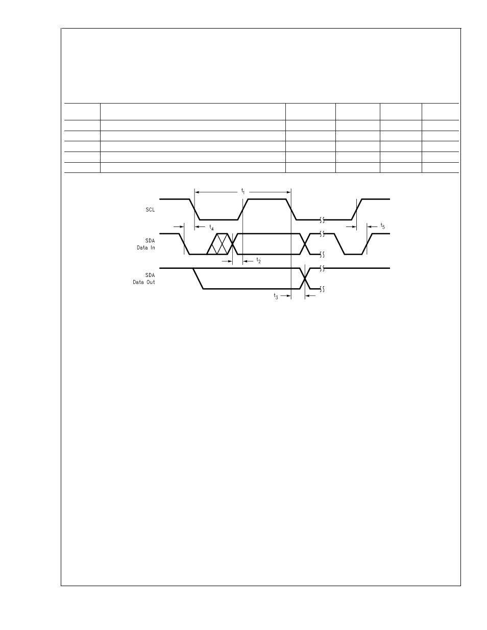
The switching characteristics of the LM77 fully meet or exceed the published specifications of the I
2
C bus. The following pa-
rameters are the timing relationship between SCL and SDA signal related to the LM77. They are not the I
2
C bus specifications.
Symbol
Parameter
Conditions
Typical
(Note 8)
Limits
(Note 9)
Units
(Limit)
t
1
SCL (Clock) Period
2.5
µs(min)
t
2
Data in Set-Up Time to SCL High
100
ns(min)
t
3
Data Out Stable after SCL Low
0
ns(min)
t
4
SDA Low Set-Up Time to SCL Low (Start Condition)
100
ns(min)
t
5
SDA High Hold Time after SCL High (Stop Condition)
100
ns(min)
Note 1: Absolute Maximum Ratings indicate limits beyond which damage to the device may occur. DC and AC electrical specifications do not apply when operating
the device beyond its rated operating conditions.
Note 2: When the input voltage (V
I
) at any pin exceeds the power supplies (V
I
<
GND or V
I
>
+V
S
) the current at that pin should be limited to 5 mA. The 20 mA
maximum package input current rating limits the number of pins that can safely exceed the power supplies with an input current of 5 mA to four.
Note 3: See AN-450 “Surface Mounting Methods and Their Effect on Product Reliability” or the section titled “Surface Mount” found in a current National
Semiconductor Linear Data Book for other methods of soldering surface mount devices.
Note 4: Human body model, 100 pF discharged through a 1.5 k
Ω
resistor. Machine model, 200 pF discharged directly into each pin.
Note 5: LM77
θ
JA
(thermal resistance, junction-to-ambient) when attached to a printed circuit board with 2 oz. foil is: 200˚C/W for the SOP-8 (M08A) package,
250˚C/W for the MSOP-8 (MUA08A) package.
Note 6: While the LM77 has a full-scale-range in excess of 128˚C, prolonged operation at temperatures above 125˚C is not recommended.
Note 7: Both part numbers of the LM77 will operate properly over the +V
S
supply voltage range of 3V to 5.5V . The devices are tested and specified for rated
accuracy at their nominal supply voltage. Accuracy will typically degrade 1˚C/V of variation in +V
S
as it varies from the nominal value.
Note 8: Typicals are at T
A
= 25˚C and represent most likely parametric norm.
Note 9: Limits are guaranteed to National’s AOQL (Average Outgoing Quality Level).
Note 10: 9 bits + sign, two’s complement
Note 11: This specification is provided only to indicate how often temperature data is updated. The LM77 can be read at any time without regard to conversion state
(and will yield last conversion result). If a conversion is in process it will be interrupted and restarted after the end of the read.
Note 12: For best accuracy, minimize output loading. Higher sink currents can affect sensor accuracy with internal heating. This can cause an error of 0.64˚C at full
rated sink current and saturation voltage based on junction-to-ambient thermal resistance.
Note 13: Hysteresis value adds to the T
LOW
setpoint value (e.g.: if T
LOW
setpoint = 10˚C, and hysteresis = 2˚C, then actual hysteresis point is 10+2 = 12˚C); and
subtracts from the T
HIGH
and T_CRIT setpoints (e.g.: if T
HIGH
setpoint = 64˚C, and hysteresis = 2˚C, then actual hysteresis point is 64−2 = 62˚C). For a detailed
discussion of the function of hysteresis refer to
Section 1.1, TEMPERATURE COMPARISON, and Figure 3.
Note 14: Default values set at power up.
DS100136-4
LM77
www.national.com
6