Absolute maximum ratings, Operating ratings, Temperature-to-digital converter characteristics – Rainbow Electronics LM77 User Manual
Page 4: Logic electrical characteristics, Lm77
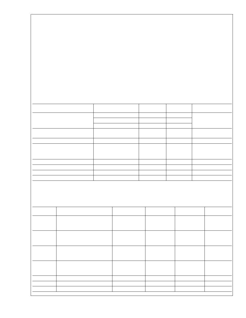
Absolute Maximum Ratings
(Note 1)
Supply Voltage
−0.3V to 6.5V
Voltage at any Pin
−0.3V to (+V
S
+ 0.3V )
Input Current at any Pin
5 mA
Package Input Current (Note 2)
20 mA
T_CRIT_A and INT Output Sink
Current
10 mA
T_CRIT_A and INT Output
Voltage
6.5V
Storage Temperature
−65˚C to +125˚C
Soldering Information, Lead
Temperature
SOP and MSOP Package (Note 3)
Vapor Phase (60 seconds)
215˚C
Infrared (15 seconds)
220˚C
ESD Susceptibility (Note 4)
Human Body Model
2500V
Machine Model
250V
Operating Ratings
(Notes 1, 5)
Specified Temperature Range
T
MIN
to T
MAX
(Note 6)
−55˚C to +125˚C
Supply Voltage Range (+V
S
)(Note 7)
+3.0V to +5.5V
Temperature-to-Digital Converter Characteristics
Unless otherwise noted, these specifications apply for +V
S
=+5 Vdc
±
10% for LM77CIM-5, LM77CIMM-5 and +V
S
=+3.3 Vdc
±
10% for LM77CIM-3, LM77CIMM-3 (Note 7). Boldface limits apply for T
A
= T
J
= T
MIN
to T
MAX
; all other limits T
A
=
T
J
=+25˚C, unless otherwise noted.
Parameter
Conditions
Typical
(Note 8)
Limits
(Note 9)
Units
(Limit)
Accuracy
T
A
= −10˚C to +65˚C
±
1.5
˚C (max)
T
A
= −25˚C to +100˚C
±
2.0
T
A
= −55˚C to +125˚C
±
3.0
Resolution
(Note 10)
10
0.5
Bits
˚C
Temperature Conversion Time
(Note 11)
70
125
ms
Quiescent Current
I
2
C Inactive
0.25
mA
I
2
C Active
0.25
0.5
mA (max)
Shutdown Mode
5
10
µA
T
HYST
Default Temperature
(Notes 13, 14)
2
˚C
T
LOW
Default Temperature
(Note 14)
10
˚C
T
HIGH
Default Temperature
(Note 14)
64
˚C
T
C
Default Temperature
(Note 14)
80
˚C
Logic Electrical Characteristics
DIGITAL DC CHARACTERISTICS Unless otherwise noted, these specifications apply for +V
S
=+5 Vdc
±
10% for LM77CIM-5,
LM77CIMM-5 and +V
S
=+3.3 Vdc
±
10% for LM77CIM-3, LM77CIMM-3. Boldface limits apply for T
A
= T
J
= T
MIN
to T
MAX
; all
other limits T
A
= T
J
=+25˚C, unless otherwise noted.
Symbol
Parameter
Conditions
Typical
(Note 8)
Limits
(Note 9)
Units
(Limit)
V
IN(1)
SDA and SCL Logical “1” Input
Voltage
+V
S
x 0.7
V (min)
+V
S
+0.3
V (max)
V
IN(0)
SDA and SCL Logical “0” Input
Voltage
−0.3
V (min)
+V
S
x 0.3
V (max)
V
IN(1)
A0 and A1 Logical “1” Input
Voltage
2.0
V (min)
+V
S
+0.3
V (max)
V
IN(0)
A0 and A1 Logical “0” Input
Voltage
−0.3
V (min)
0.8
V (max)
I
IN(1)
Logical “1” Input Current
V
IN
= + V
S
0.005
1.0
µA (max)
I
IN(0)
Logical “0” Input Current
V
IN
= 0V
−0.005
−1.0
µA (max)
C
IN
Capacitance of All Digital Inputs
20
pF
LM77
www.national.com
4