Applications information – Rainbow Electronics MAX998 User Manual
Page 6
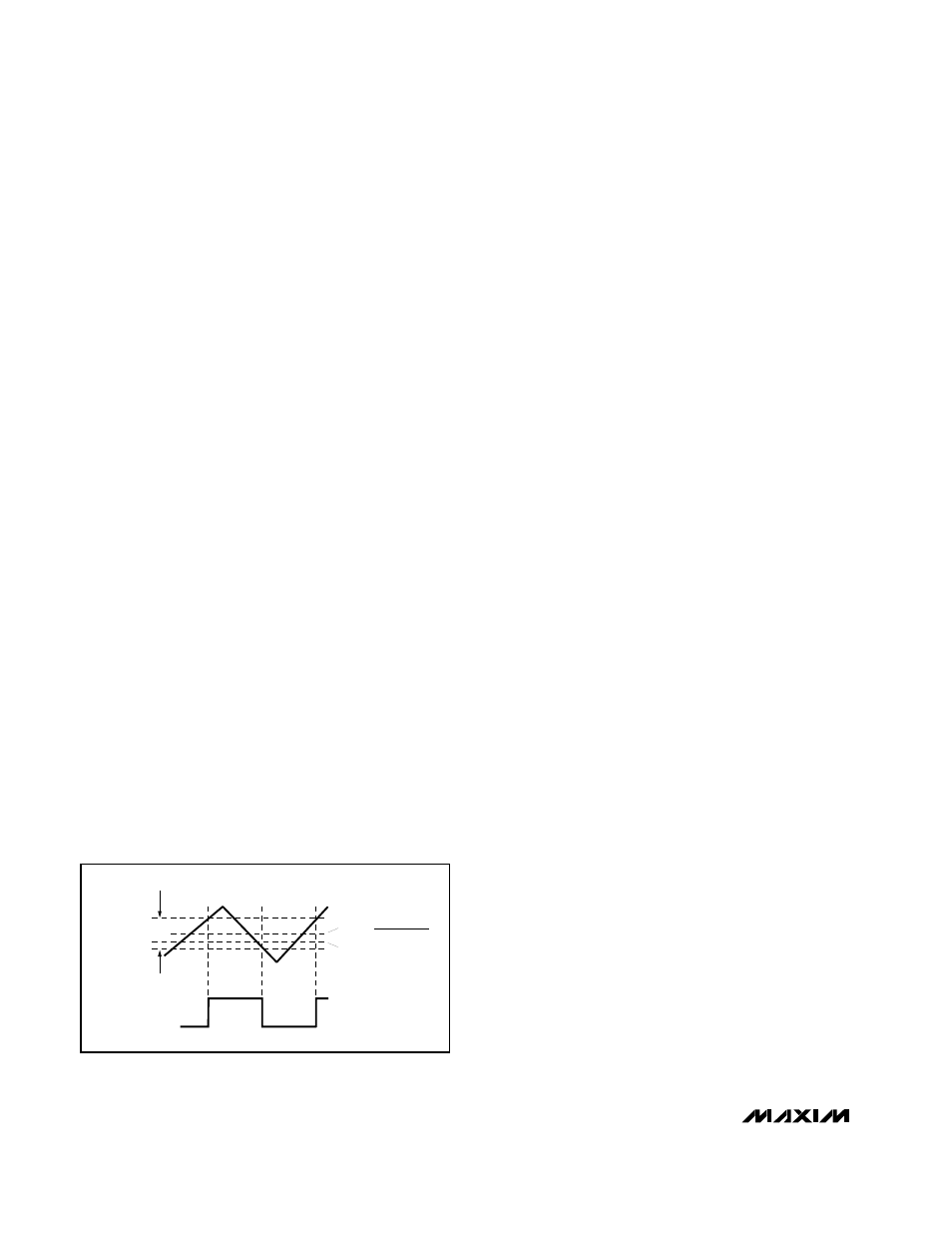
Hysteresis
High-speed comparators can oscillate in the linear
operating region because of noise or undesired para-
sitic feedback. This tends to occur when the voltage on
one input is equal to or very close to the voltage on the
other input. The MAX976/MAX978/MAX998 have inter-
nal hysteresis to counter parasitic effects and noise.
The hysteresis in a comparator creates two trip points:
one for the rising input voltage and one for the falling
input voltage (Figure 1). The difference between the trip
points is the hysteresis. When the comparator input
voltages are equal, the hysteresis effectively causes
one comparator input voltage to move quickly past the
other, taking the input out of the region where oscilla-
tion occurs.
Figure 1 illustrates the case where IN- has a fixed volt-
age applied and IN+ is varied. If the inputs were
reversed, the figure would be the same, except with an
inverted output.
Input-Stage Circuitry
The MAX976/MAX978/MAX998 input common-mode
voltage range is from -0.2V to (V
CC
- 1.2V). The voltage
range for each comparator input extends to both V
CC
and GND. The output remains in the correct logic state
while one or both of the inputs are within the common-
mode range. If both input levels are out of the common-
mode range, input-stage current saturation occurs, and
the output becomes unpredictable.
Shutdown Mode
The MAX998 features a low-power shutdown mode,
which is activated by forcing SHDN low. Shutdown
mode reduces the supply current to 1nA (typical), dis-
ables the comparator, and places the output in a high-
impedance state. Drive SHDN high to enable the
comparator. Do not leave SHDN unconnected. Since it
is a high-impedance input, leaving SHDN unconnected
could result in indeterminate logic levels, adversely
affecting comparator operation. Likewise, do not three-
state SHDN. Due to the output leakage currents of
three-state devices and the small internal current for
SHDN, three-stating this pin could also result in indeter-
minate logic levels.
The maximum input voltage for SHDN is 6V, referred to
GND, and is not limited by V
CC
. This allows the use of
5V logic to drive SHDN while V
CC
operates at a lower
voltage, such as 3V. The logic threshold limits for
SHDN are proportional to V
CC
(see
Electrical
Characteristics
).
_____________Applications Information
Circuit Layout and Bypassing
The MAX976/MAX978/MAX998 have a high-gain band-
width and require careful board layout. We recommend
the following design guidelines:
1) Use a printed circuit board with an unbroken, low-
inductance ground plane. Surface-mount compo-
nents are recommended.
2) Place a decoupling capacitor (a 0.1µF ceramic
capacitor is a good choice) between V
CC
and
ground as close to the pins as possible.
3) Keep lead lengths short on the inputs and outputs
to avoid unwanted parasitic feedback around the
comparators.
4) Solder the devices directly to the printed circuit
board instead of using a socket.
5) Minimize input impedance.
6) For slowly varying inputs, use a small capacitor
(~1000pF) across the inputs to improve stability.
Additional Hysteresis
Generate additional hysteresis with three resistors
using positive feedback, as shown in Figure 2. This
positive feedback method slows the hysteresis
response time. Calculate resistor values as follows:
1) Select R3. The leakage current of IN+ is typically
75nA, so the current through R3 should be at least
1.0µA to minimize errors caused by leakage current.
The current through R3 at the trip point is (V
REF
-
V
OUT
) / R3. Consider the two possible output states
when solving for R3. The two formulas are:
R3 = V
REF
/ 1.0µA
or
R3 = (V
CC
- V
REF
) / 1.0µA
Use the smaller of the two resulting resistor values.
For example, if V
REF
= 1.2V and V
CC
= 5.0V, the two
resistor values are 1.2M
Ω
and 3.8M
Ω
. Choose a
standard value for R3 of 1.2M
Ω
.
MAX976/MAX978/MAX998
Single/Dual/Quad, SOT23, Single-Supply,
High-Speed, Low-Power Comparators
6
_______________________________________________________________________________________
V
OL
V
OH
V
IN-
= 0
V
OS
=
V
TRIP+
+ V
TRIP-
2
COMPARATOR
OUTPUT
V
TRIP+
V
IN+
V
HYST
V
TRIP-
Figure 1. Input and Output Waveforms, Noninverting Input
Varied