Rainbow Electronics MAX1116 User Manual
Page 9
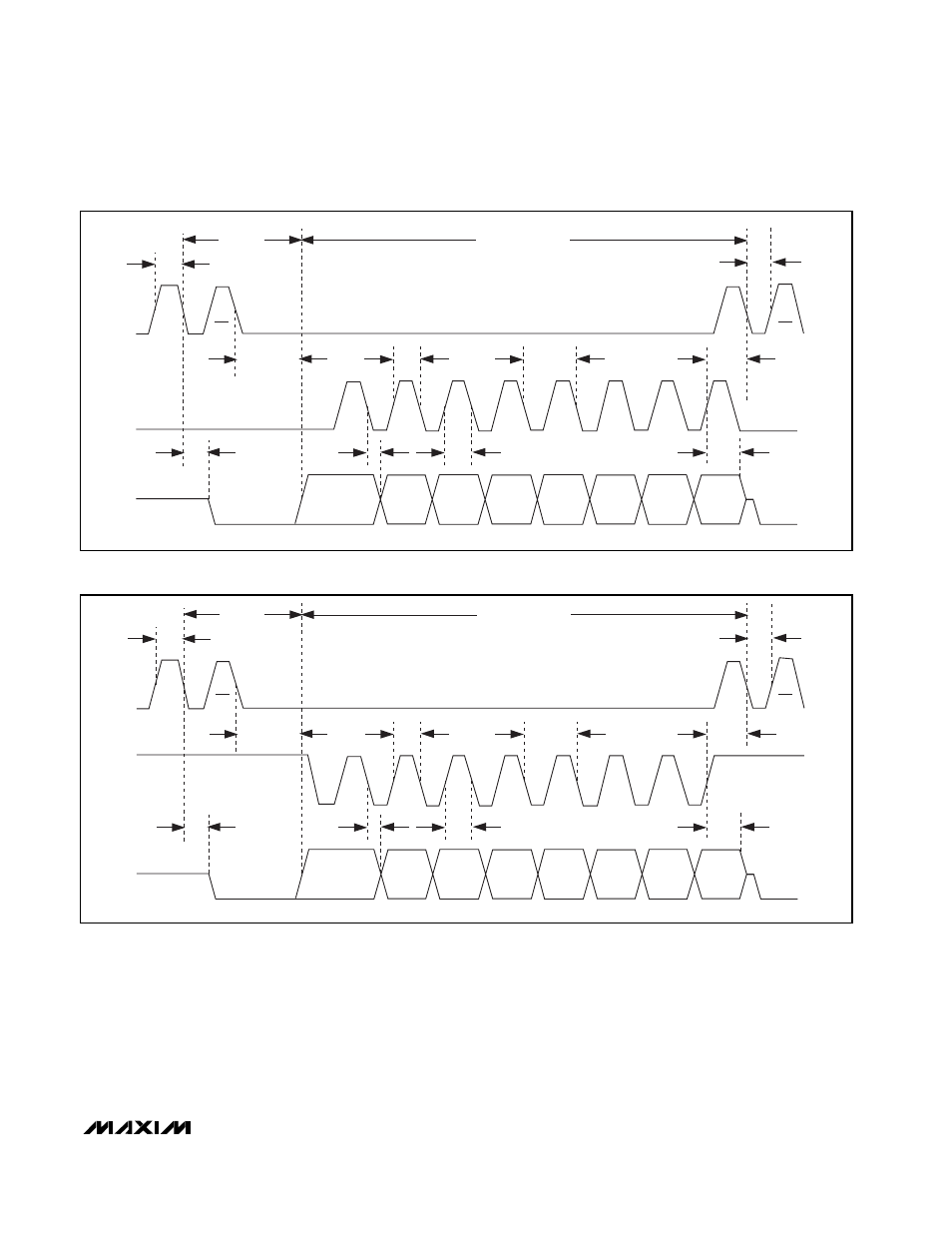
After CNVST is brought low, allow 7.5µs for the conver-
sion to be completed. While the internal conversion is in
progress, DOUT is low. The MSB is present at the
DOUT pin immediately after conversion is completed.
The conversion result is clocked out at the DOUT pin
and is coded in straight binary (Figure 7). Data is
clocked out at SCLK’s falling edge in MSB-first format
at rates up to 5MHz. Once all data bits are clocked out,
DOUT goes high impedance (100ns to 500ns after the
rising edge) of the eighth SCLK pulse.
SCLK is ignored during the conversion process. Only
after a conversion is complete will SCLK cause serial
data to be output. Falling edges on CNVST during an
MAX1115/MAX1116
Single-Supply, Low-Power, Serial 8-Bit ADCs
_______________________________________________________________________________________
9
ACTIVE
POWER-DOWN MODE
CNVST
SCLK
DOUT
CH0
IDLE LOW
IDLE LOW
CH0
t
CSH
t
CONV
t
cp
t
ccs
t
CSL
t
chz
t
cl
t
cd
D7 (MSB)
D6
D5
D4
D3
D2
D1
D0
t
csd
t
ch
V
DD
2
V
DD
2
Figure 6c. Conversion and Interface Timing, Conversion on V
DD
/ 2 with SCLK Idle Low
ACTIVE
POWER-DOWN MODE
CNVST
SCLK
DOUT
CH0
IDLE HIGH
IDLE HIGH
CH0
t
CSH
t
CONV
t
cp
t
ccs
t
csl
t
chz
t
cl
t
cd
D7 (MSB)
D6
D5
D4
D3
D2
D1
D0
t
csd
t
ch
V
DD
2
V
DD
2
Figure 6d. Conversion and Interface Timing, Conversion on V
DD
/ 2 with SCLK Idle High