Single-supply, low-power, serial 8-bit adcs, Digital inputs and outputs – Rainbow Electronics MAX1116 User Manual
Page 8
MAX1115/MAX1116
Digital Inputs and Outputs
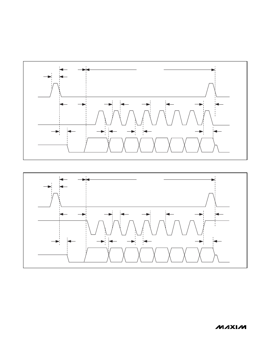
The MAX1115/MAX1116 perform conversions by using
an internal clock. This frees the µP from the burden of
running the SAR conversion clock, and allows the con-
version results to be read back at the µP’s convenience
at any clock rate up to 5MHz.
The acquisition interval begins with the falling edge of
CNVST. CNVST can idle between conversions in either
a high or low state. If idled in a low state, CNVST must
be brought high for at least 50ns, then brought low to
initiate a conversion. To select V
DD
/2 for conversion,
the CNVST pin must be brought high and low for a sec-
ond time (Figures 6c and 6d).
Single-Supply, Low-Power, Serial 8-Bit ADCs
8
_______________________________________________________________________________________
ACTIVE
POWER-DOWN MODE
CNVST
SCLK
DOUT
CH0
IDLE LOW
IDLE LOW
CH0
t
CSH
t
CONV
t
cp
t
ccs
t
chz
t
cl
t
cd
D7 (MSB)
D6
D5
D4
D3
D2
D1
D0
t
csd
t
ch
Figure 6a. Conversion and Interface Timing, Conversion on CH0 with SCLK Idle Low
ACTIVE
POWER-DOWN MODE
CNVST
SCLK
DOUT
CH0
IDLE HIGH
IDLE HIGH
CH0
t
CSH
t
CONV
t
cp
t
ccs
t
chz
t
cl
t
cd
D7 (MSB)
D6
D5
D4
D3
D2
D1
D0
t
csd
t
ch
Figure 6b. Conversion and Interface Timing, Conversion on CH0 with SCLK Idle High