Single-supply, low-power, serial 8-bit adcs, Applications information – Rainbow Electronics MAX1116 User Manual
Page 10
MAX1115/MAX1116
active conversion process interrupt the current conver-
sion and cause the input multiplexer to switch to V
DD
/2.
To reinitiate a conversion on CH0, it is necessary to allow
for a conversion to be complete and all of the data to be
read out. Once a conversion has been completed, the
MAX1115/MAX1116 will go into Autoshutdown mode
(typically <1µA) until the next conversion is initiated.
Applications Information
Power-On Reset
When power is first applied, the MAX1115/MAX1116
are in AutoShutdown (typically <1µA). A conversion
can be started by toggling CNVST high to low.
Powering up the MAX1115/MAX1116 with CNVST low
will not start a conversion.
AutoShutdown and Supply Current
Requirements
The MAX1115/MAX1116 are designed to automatically
shutdown once a conversion is complete, without any
external control. An input sample and conversion
process will typically take 5µs to complete, during
which time the supply current to the analog sections of
the device are fully on. All analog circuitry is shutdown
after a conversion completes, which results in a supply
current of <1µA (see Shutdown Current vs. Supply Volt-
age plot in the Typical Operating Characteristics sec-
tion). The digital conversion result is maintained in a
static register and is available for access through the
serial interface at any time.
The power consumption consequence of this architec-
ture is dramatic when relatively slow conversion rates
are needed. For example, at a conversion rate of
10ksps, the average supply current for the MAX1115 is
15µA, while at 1ksps it drops to 15µA. At 0.1 ksps it is
just 0.3µA, or a miniscule 1µW of power consumption
(see Average Supply Current vs. Conversion Rate plot
in the Typical Operating Characteristics sections).
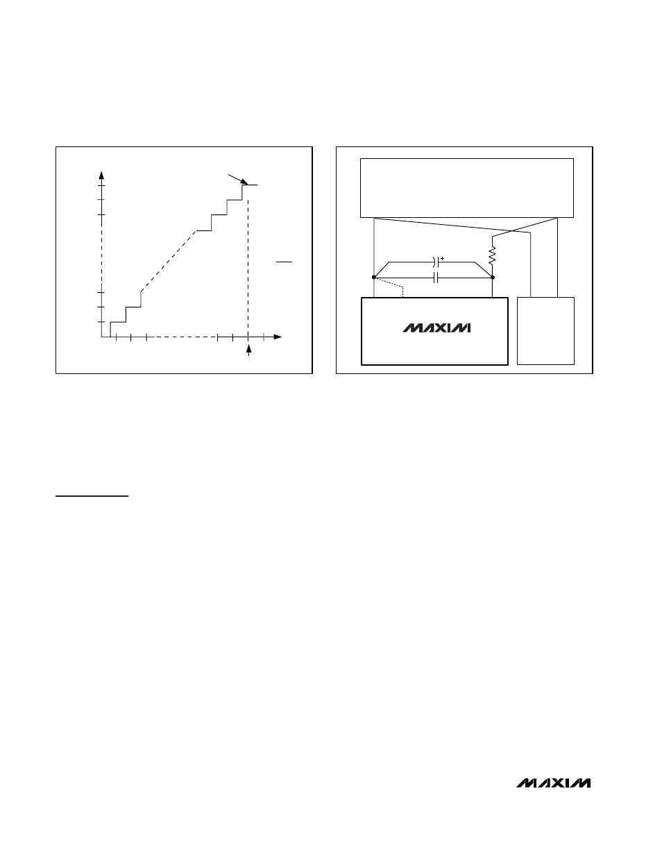
Transfer Function
Figure 7 depicts the input/output transfer function.
Output coding is binary with a +2.048V reference,
1LSB = 8mV(V
REF
/256).
Layout, Grounding, and Bypassing
For best performance, board layout should ensure that
digital and analog signal lines are separated from each
other. Do not run analog and digital (especially clock)
lines parallel to one another or run digital lines under-
neath the ADC package.
Figure 8 shows the recommended system-ground con-
nections. A single-point analog ground (star-ground
point) should be established at the ADC ground.
Connect all analog grounds to the star-ground. The
ground-return to the power supply for the star ground
should be low impedance and as short as possible for
noise-free operation.
High-frequency noise in the V
DD
power supply may
affect the comparator in the ADC. Bypass the supply to
the star ground with a 0.1µF capacitor close to the V
DD
pin of the MAX1115/MAX1116. Minimize capacitor lead
Single-Supply, Low-Power, Serial 8-Bit ADCs
10
______________________________________________________________________________________
OUTPUT CODE
FULL-SCALE
TRANSITION
11111111
11111110
11111101
00000011
00000010
00000001
00000000
1
2
3
0
FS
FS - 1/2 LSB
FS = V
REFIN
+ V
IN-
1LSB = V
REFIN
256
INPUT VOLTAGE (LSB)
Figure 7. Input/Output Transfer Function
GND
+3V/+5V
SYSTEM POWER SUPPLIES
V
DD
DGND
V
DD
IN-
1
µF
10
Ω
0.1
µF
GND
DIGITAL
CIRCUITRY
MAX1115
MAX1116
Figure 8. Power-Supply Connections