Applications information, Chip information – Rainbow Electronics MAX868 User Manual
Page 8
MAX868
Regulated, Adjustable -2x
Inverting Charge Pump
8
___________________________________
__________Applications Information
Low-Output-Voltage Operation
Since the difference between the voltage of the series-
connected flying capacitors and the output voltage
must be dissipated within the device, the MAX868’s
efficiency is very similar to that of a linear regulator.
Estimate efficiency using the following equation:
where k is a constant equal to 2 for the standard con-
figuration of Figure 5 and equal to 1 for the circuit of
Figure 6. This equation’s denominator is the voltage
resulting from the series connection of the flying capac-
itors (-2 x V
IN
, as shown in Figure 3b), while its numera-
tor is simply the regulated output voltage.
For applications in which the output voltage will not be
more negative than -
|
V
IN
|
, the efficiency can be doubled
using the circuit of Figure 6, as compared to the circuit
of Figure 5. In Figure 6, a single flying capacitor is con-
nected between C2+ and C1-, with C2- and C1+ left
unconnected. Furthermore, doubling the flying capaci-
tor to provide the same flying capacitance as the stan-
dard configuration (i.e., setting C
F
= C1 + C2) provides
the same load-current capability as the standard con-
figuration and reduces the MAX868’s open-loop output
resistance by a factor of two, due to the reduction in the
number of switches in the current path.
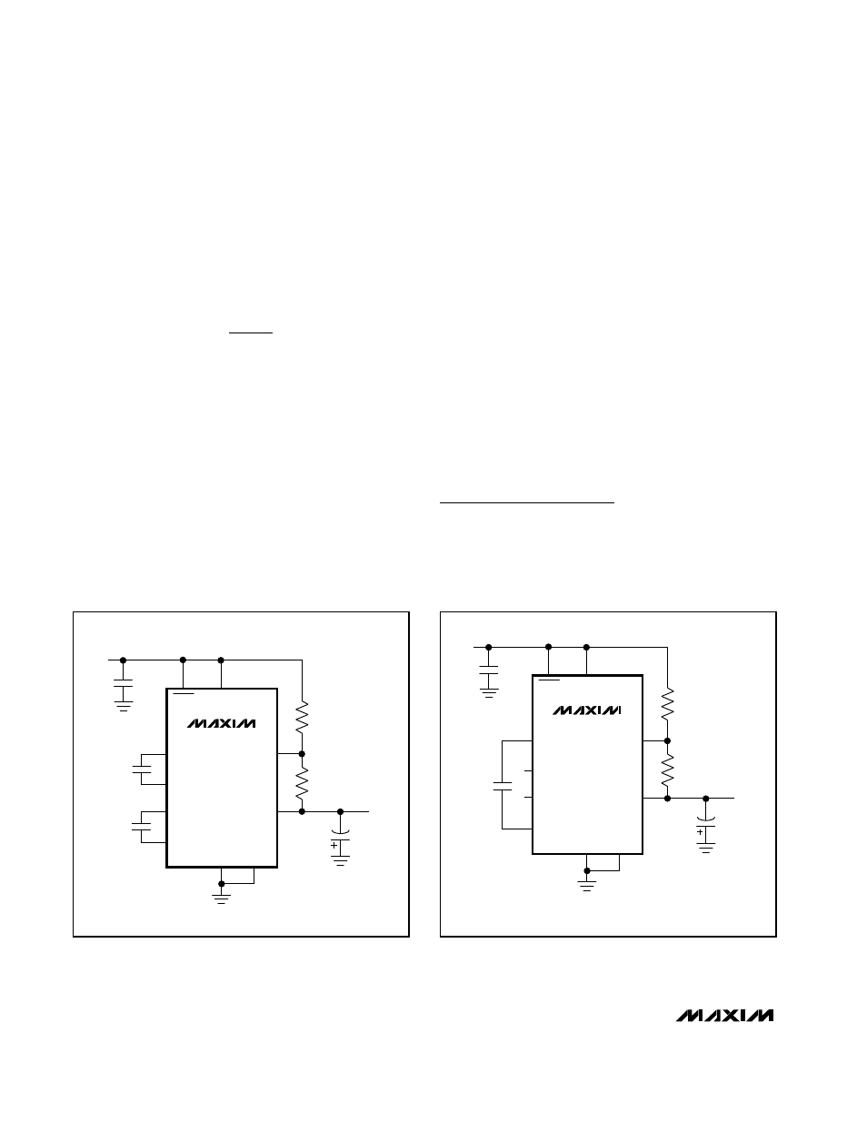
Layout and Grounding
Proper layout is important to obtain optimal perfor-
mance. Connect GND to PGND together using the
shortest trace possible, and similarly connect these
pins to the ground plane. Mount all capacitors as close
to the MAX868 as possible, keeping traces short to
minimize parasitics. Keep all connections to the FB pin
as short as possible. Specifically, locate R1 and R2
next to FB (Figures 7 and 8). Should it become neces-
sary in the final layout, leave room to parallel a feed-
forward capacitor across R1.
η
V
k x V
|
|
OUT
IN
=
MAX868
C1+
IN
PGND
SHDN
GND
FB
R2
500k
R1
750k
OUT
0.1
µ
F
1
µ
F
10
µ
F
V
OUT
= -7.5V
V
IN
= 5V
0.1
µ
F
C1-
C2+
C2-
Figure 5. Standard Configuration for Generating an Output
Voltage up to -2 x V
IN
MAX868
C2+
IN
PGND
SHDN
GND
FB
OUT
C
F
= 0.2
µ
F
*
*
1
µ
F
10
µ
F
V
OUT
= -3.3V
AT 20mA
V
IN
= 5V
C2-
C1+
C1-
*C1+ AND C2- MUST BE LEFT UNCONNECTED.
R2
500k
R1
330k
Figure 6. Alternative Configuration for
|
V
OUT
|
≤
V
IN
Chip Information
TRANSISTOR COUNT: 96
SUBSTRATE CONNECTED TO IN