Detailed description, Pin description – Rainbow Electronics MAX868 User Manual
Page 5
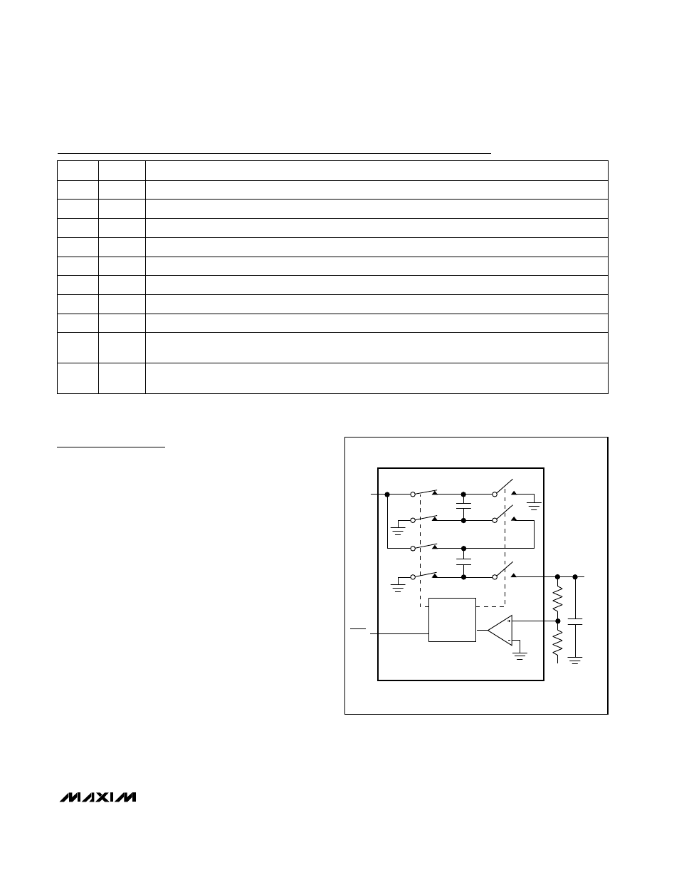
Detailed Description
The MAX868 inverting charge pump uses pulse-
frequency-modulation (PFM) control to generate a reg-
ulated negative output voltage up to -2 x V
IN
. PFM
operation is obtained by enabling the internal 450kHz
oscillator as needed to maintain output voltage regula-
tion. This control scheme reduces supply current at
light loads and permits the use of small capacitors.
The functional diagram shown in Figure 1 indicates the
two phases of MAX868 operation: charge phase (
Φ
1)
and discharge phase (
Φ
2). In charge phase, the
switches on the left-hand side close, and the switches
on the right-hand side open. In the discharge phase,
the inverse occurs.
Figure 2 illustrates that in charge phase, both flying
capacitors are charged in parallel. The load is serviced
entirely by the charge stored in the output capacitor.
Figure 3 demonstrates the series connection of the fly-
ing capacitors in the discharge phase. The series com-
bination of the flying capacitors, when connected to the
output capacitor, transfers charge to the output in order
to maintain output voltage regulation. In normal opera-
tion, the MAX868 operates predominantly in charge
phase, switching to discharge phase only as needed to
maintain a regulated output.
MAX868
Regulated, Adjustable -2x
Inverting Charge Pump
_______________________________________________________________________________________
5
Pin Description
Active-Low Shutdown Input. Connect SHDN to GND to put the MAX868 in shutdown mode and reduce sup-
ply current to 0.1µA. Connect to IN for normal operation. OUT is actively pulled to GND in shutdown.
SHDN
9
Feedback Input. Connect FB to a resistor divider for a regulated output voltage. Connect to IN to generate
an unregulated -2 x V
IN
output voltage.
FB
10
Positive Terminal of Flying Capacitor C1
C1+
5
Negative Terminal of Flying Capacitor C2
C2-
6
Supply-Voltage Input. Input voltage range is 1.8V to 5.5V.
IN
7
Positive Terminal of Flying Capacitor C2
C2+
8
Power Ground
PGND
4
Negative Terminal of Flying Capacitor C1
C1-
3
PIN
Charge-Pump Output
OUT
2
Analog Ground
GND
1
FUNCTION
NAME
V
REF
C
OUT
OUT
C2-
C1+
C1-
FB
Φ
1
Φ
2
OSCILLATOR
C2+
IN
SHDN
Figure 1. Functional Diagram