Max868, Regulated, adjustable -2x inverting charge pump, Design procedure – Rainbow Electronics MAX868 User Manual
Page 6
MAX868
__________________Design Procedure
Setting the Output Voltage
Set the output voltage using two external resistors, R1
and R2, as shown in Figure 4. Since the input bias cur-
rent at FB has a 50nA maximum, large resistor values in
the feedback loop do not significantly degrade accura-
cy. Begin by selecting R2 in the 100k
Ω
to 500k
Ω
range,
and calculate R1 using the following equation:
where V
OUT
is the desired output voltage, and V
REF
is
any available regulated positive voltage. When the
MAX868 is powered by a regulated voltage, V
IN
can be
used as the reference for setting the output voltage.
When the MAX868 is powered by an unregulated sup-
ply, such as when operating directly from a battery, use
any available positive reference voltage in the system.
Note that due to the MAX868’s doubling and inverting
charge-pump action, the output voltage is limited to
-2 x V
IN
.
Alternatively, to configure the MAX868 as a simple,
unregulated doubler-inverter (V
OUT
= -2 x V
IN
), con-
nect FB to IN. In this configuration, the MAX868 runs at
its maximum oscillator frequency, operating as a con-
ventional, open-loop charge pump.
If multiple oscillator cycles are required to regulate the
output, reduce the values for R1 and R2, or parallel a
small capacitor (C
C
) across R1 to compensate the
feedback loop and ensure stability. Choose the lowest
capacitor value that ensures stability; values up to 47pF
are adequate for most applications.
R
R
x
V
V
OUT
REF
1
2
|
|
=
Regulated, Adjustable -2x
Inverting Charge Pump
6
_______________________________________________________________________________________
C
OUT
V
OUT
C2-
C1+
C1-
C2+
IN
IN
GND
(a)
(b)
C
OUT
V
OUT
C2-
C2+
C1-
C1+
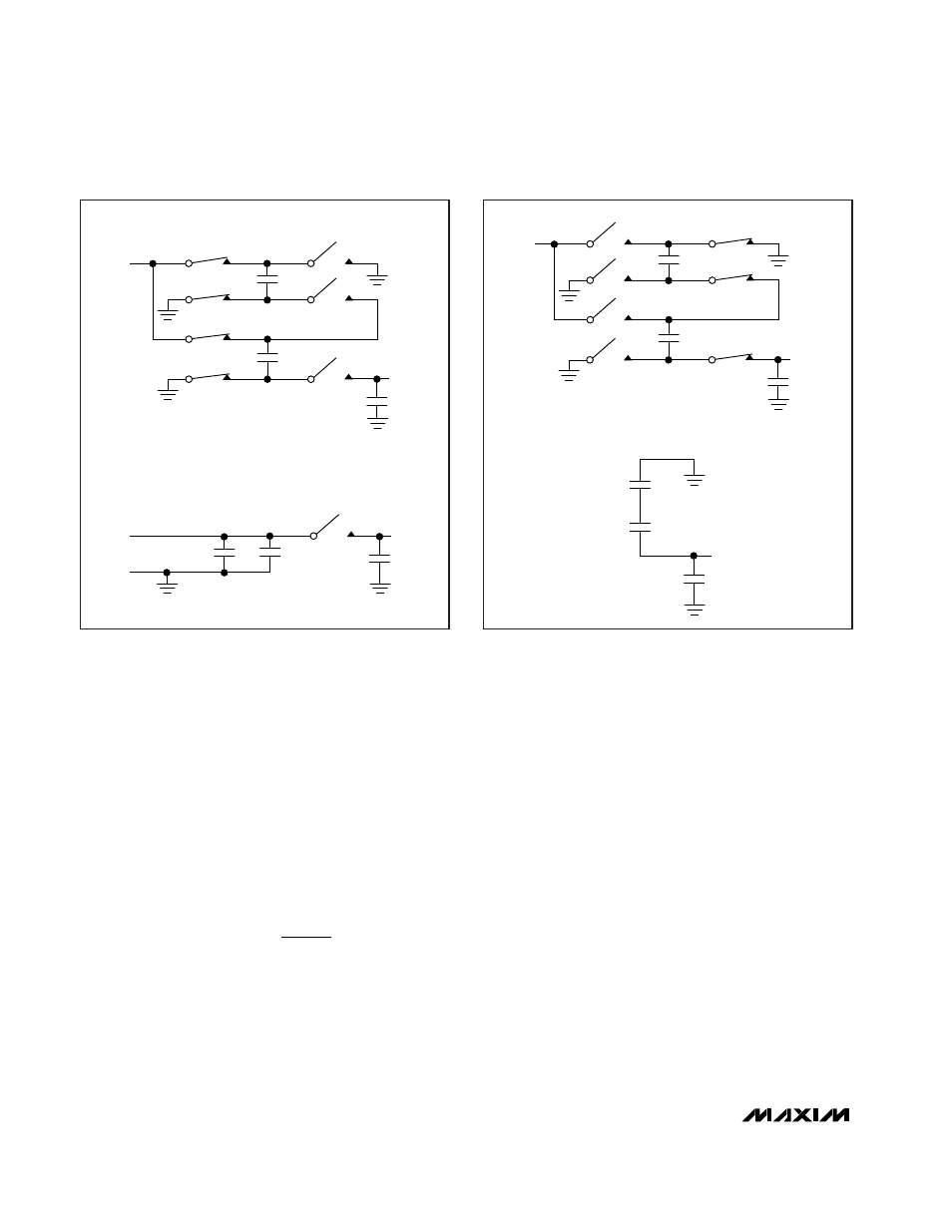
Figure 2.
a)
In charge phase, the left-hand switches are
closed and the right-hand switches are open, charging the fly-
ing capacitors (C1 and C2) while the output capacitor (C
OUT
)
services the load.
b)
The equivalent circuit of the charge phase
of operation.
C2-
C1+
C1-
C2+
IN
(a)
(b)
C
OUT
V
OUT
C
OUT
V
OUT
C2+
C2-
C1+
C1-
Figure 3.
a)
In discharge phase, the left-hand switches are
open and the right-hand switches are closed, transferring
energy from the flying capacitors (C1 and C2) to the output
capacitor (C
OUT
).
b)
The equivalent circuit of the discharge
phase of operation.