Max2203 rms power detector, Ac electrical characteristics – Rainbow Electronics MAX2203 User Manual
Page 2

MAX2203
RMS Power Detector
2
_______________________________________________________________________________________
ABSOLUTE MAXIMUM RATINGS
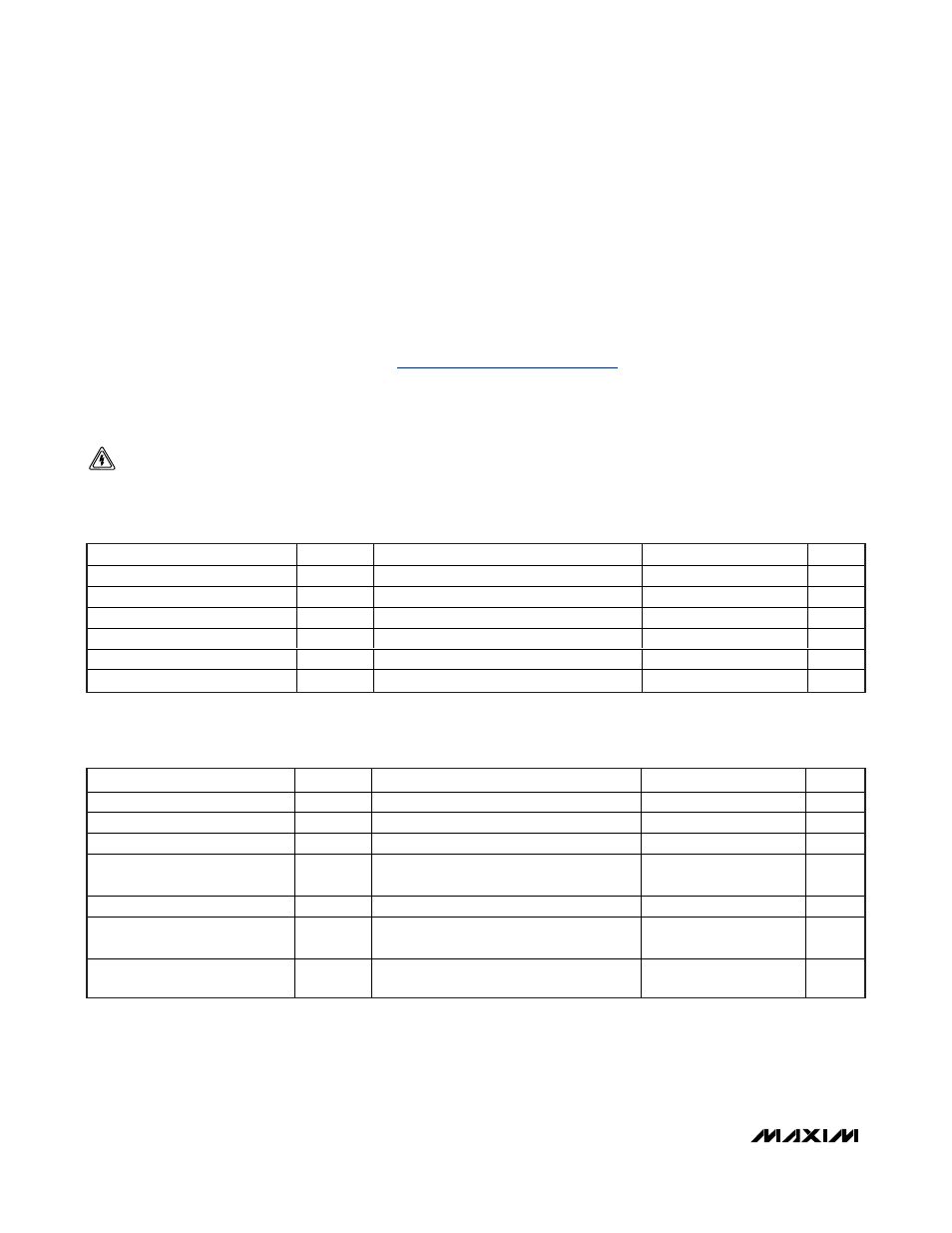
DC ELECTRICAL CHARACTERISTICS
(V
CC
= 2.5V to 4.2V, T
A
= -40°C to +85°C, V
ENA
= 2.7V, no RF signal applied. Typical values are at V
CC
= 2.8V, T
A
= +25°C, unless
otherwise noted.) (Note 3)
Stresses beyond those listed under “Absolute Maximum Ratings” may cause permanent damage to the device. These are stress ratings only, and functional
operation of the device at these or any other conditions beyond those indicated in the operational sections of the specifications is not implied. Exposure to
absolute maximum rating conditions for extended periods may affect device reliability.
Note 3: Guaranteed by production test at T
A
= +85°C and 800MHz. Guaranteed by design and characterization at T
A
= -40°C and
T
A
= +25°C, and over frequency limits.
Note 4: Guaranteed by design and characterization.
Note 5: Input power -24dBm to +3dBm. Ideal straight line calibrated with input power -20dBm and 0dBm at T
A
= +25°C.
V
CC
to GND ...........................................................-0.3V to +4.5V
ENA, OUT, FILT to GND ........................................-0.3V to +3.0V
RFIN Input Power ...........................................................+10dBm
Continuous Power Dissipation (T
A
= +70
°C)
6-Bump WLP (derate 2.9mW/
°C above +70°C)...........232mW
Junction-to-Ambient Thermal Resistance (
θ
JA
)
(Note 1) ......................................................................347°C/W
Operating Temperature Range ...........................-40
°C to +85°C
Storage Temperature Range .............................-65
°C to +160°C
Junction Temperature .....................................................+150
°C
Lead Temperature (soldering, 10s)..........Reflow Profile (Note 2)
PARAMETER
SYMBOL
CONDITIONS
MIN
TYP
MAX
UNITS
Supply Voltage
V
CC
2.5
2.8
4.2
V
Supply Current
I
CC
V
CC
= 2.8V, RF input = -24dBm to +3dBm
5
8
mA
Shutdown Supply Current
V
ENA
= 0V
0.5
10
µA
ENA Logic-High Threshold
V
IH
1.1
2.7
V
ENA Logic-Low Threshold
V
IL
0
0.6
V
ENA Input Current
V
ENA
= 1.1V
25
µA
AC ELECTRICAL CHARACTERISTICS
(V
CC
= 2.8V, T
A
= -40°C to +85°C, V
ENA
= 2.7V, f
RF
= 800MHz to 2GHz, unless otherwise noted. Typical values are at T
A
= +25°C.)
(Note 3)
PARAMETER
SYMBOL
CONDITIONS
MIN
TYP
MAX
UNITS
RF Input Frequency
800
2000
MHz
Maximum Output Voltage
RFIN at +3dBm
1.05
1.5
1.75
V
Minimum Output Voltage
No RF input power
300
400
mV
Minimum Input Power Level
+1dB input power step results in at least
25mV increase in V
OUT
(Note 4)
-24 dBm
Log Slope
[(V
OUT
at +3dBm) - (V
OUT
at
-24dBm)]/27 25 35 45
mV/dB
Log Conformance Error with
10dB Step
(Notes 4, 5)
-1.3
+1.3
dB
Power-Detector Accuracy Due to
Temperature
RF input at -4dBm to 0dBm, T
A
= -40
°C to
+85
°C, relative to +25°C
±0.4 dB
Note 1: Package thermal resistances were obtained using the method described in JEDEC specifications. For detailed information
on package thermal considerations, refer to
www.maxim-ic.com/thermal-tutorial
.
Note 2: Refer to Application Note 1891:
Wafer-Level Packaging (WLP) and Its Applications.
CAUTION! ESD SENSITIVE DEVICE
