Typical operating characteristics (continued), Pin description – Rainbow Electronics MAX3469 User Manual
Page 6

MAX3465–MAX3469
+5V, Fail-Safe, 40Mbps, Profibus RS-485/
RS-422 Transceivers
6
_______________________________________________________________________________________
Typical Operating Characteristics (continued)
(V
CC
= +5V, T
A
= +25°C, unless otherwise noted.)
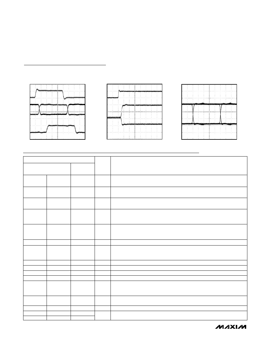
DRIVER AND RECEIVER
PROPAGATION DELAYS
MAX3465 toc13
10ns/div
5V/div
5V/div
2V/div
Y, Z
DI
RO
R
DIFF
= 54
Ω
DATA RATE = 20Mbps
ENABLE RESPONSE TIME
MAX3465 toc14
20ns/div
5V/div
1V/div
Y, Z
DE
R
DIFF
= 54
Ω
EYE DIAGRAM
MAX3465 toc15
10ns/div
1V/div
Y, Z
R
DIFF
= 54
Ω
DATA RATE = 20Mbps
Pin Description
PIN
FULL DUPLEX
HALF
DUPLEX
NAME
FUNCTION
MAX3465/
MAX3466
MAX3467
MAX3468/
MAX3469
SHDN
Shutdown. Drive SHDN high to enter low-power shutdown mode.
1
—
—
RO
Receiver Output. When RE is low and (A - B)
≥ -50mV, RO is high; if (A - B) ≤
-200mV, RO is low.
2
2
1
RE
Receiver Output Enable. Drive RE low to enable RO; RO is high impedance
when RE is high. Drive RE high and DE low to enter low-power shutdown mode.
3
—
2
DE
Driver Output Enable. Drive DE high to enable driver output. The driver
outputs are high impedance when DE is low. Drive RE high and DE low to
enter low-power shutdown mode.
4
—
3
DI
Driver Input. With DE high, a low on DI forces the noninverting output low and
the inverting output high. Similarly, a high on DI forces the noninverting output
high and the inverting output low.
5
3
4
GND
Ground
6, 7
4
5
TXP
Transmitter Phase. Connect TXP to GND, or leave unconnected for normal
transmitter phase/polarity. Connect TXP to V
CC
to invert the transmitter
phase/polarity. TXP has an internal 15µA pulldown.
8
—
—
Y
Noninverting Driver Output
9
5
—
Z
Inverting Driver Output
10
6
—
B
Inverting Receiver Input
11
7
—
A
Noninverting Receiver Input
12
8
—
RXP
Receiver Phase. Connect RXP to GND, or leave unconnected for normal
receiver phase/polarity. Connect RXP to V
CC
to invert the receiver
phase/polarity. RXP has an internal 15µA pulldown.
13
—
—
V
CC
Positive Supply: +4.75V
≤ V
CC
≤ +5.25V. Bypass V
CC
to GND with a 0.1µF
capacitor.
14
1
8
B
Inverting Receiver Input and Inverting Driver Output
—
—
7
A
Noninverting Receiver Input and Noninverting Driver Output
—
—
6
