Absolute maximum ratings, Operating ratings, Electrical characteristics – Rainbow Electronics LM62 User Manual
Page 2: Lm62
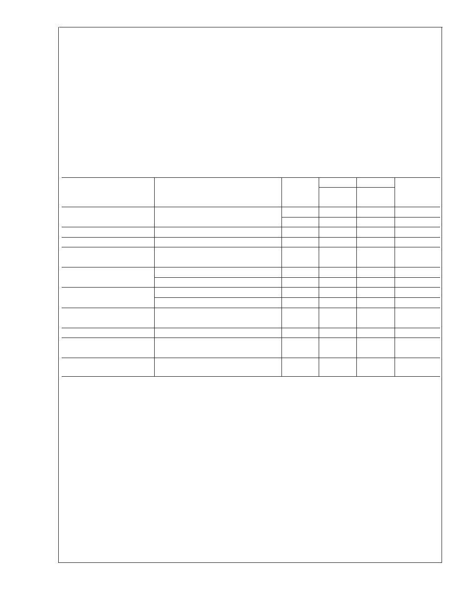
Absolute Maximum Ratings
(Note 1)
Supply Voltage
+12V to −0.2V
Output Voltage
(+V
S
+ 0.6V) to
−0.6V
Output Current
10 mA
Input Current at any pin (Note 2)
5 mA
Storage Temperature
−65˚C to +150˚C
Maximum Junction Temperature (T
JMAX
)
+125˚C
ESD Susceptibility (Note 3) :
Human Body Model
2500V
Machine Model
250V
Lead Temperature:
SOT Package (Note 4) :
Vapor Phase (60 seconds)
+215˚C
Infrared (15 seconds)
+220˚C
Operating Ratings
(Note 1)
Specified Temperature Range:
T
MIN
≤
T
A
≤
T
MAX
LM62B, LM62C
0˚C
≤
T
A
≤
+90˚C
Supply Voltage Range (+V
S
)
+2.7V to +10V
Thermal Resistance,
θ
JA
(Note 5)
450˚C/W
Electrical Characteristics
Unless otherwise noted, these specifications apply for +V
S
= +3.0 V
DC
. Boldface limits apply for T
A
= T
J
= T
MIN
to T
MAX
; all
other limits T
A
= T
J
= 25˚C.
Parameter
Conditions
Typical
(Note 6)
LM62B
LM62C
Units
(Limit)
Limits
Limits
(Note 7)
(Note 7)
Accuracy (Note 8)
±
2.0
±
3.0
˚C (max)
+2.5/−2.0
+4.0/−3.0
˚C (max)
Output Voltage at 0˚C
+480
mV
Nonlinearity (Note 9)
±
0.8
±
1.0
˚C (max)
Sensor Gain
+16
+16.1
+16.3
mV/˚C (max)
(Average Slope)
+15.1
+14.9
mV/˚C (min)
Output Impedance
+3.0V
≤
+V
S
≤
+10V
4.7
4.7
k
Ω
(max)
0˚C
≤
T
A
≤
+75˚C, +V
S
= +2.7V
4.4
4.4
k
Ω
(max)
Line Regulation (Note 10)
+3.0V
≤
+V
S
≤
+10V
±
1.13
±
1.13
mV/V (max)
+2.7V
≤
+V
S
≤
+3.3V, 0˚C
≤
T
A
≤
+75˚C
±
9.7
±
9.7
mV (max)
Quiescent Current
+2.7V
≤
+V
S
≤
+10V
82
130
130
µA (max)
165
165
µA (max)
Change of Quiescent Current
+2.7V
≤
+V
S
≤
+10V
±
5
µA
Temperature Coefficient of
0.2
µA/˚C
Quiescent Current
Long Term Stability (Note 11)
T
J
=T
MAX
=+100˚C,
for 1000 hours
±
0.2
˚C
Note 1: Absolute Maximum Ratings indicate limits beyond which damage to the device may occur. Operating Ratings indicate conditions for which the device is
functional, but do not guarantee specific performance limits. For guaranteed specifications and test conditions, see the Electrical Characteristics. The guaranteed
specifications apply only for the test conditions listed. Some performance characteristics may degrade when the device is not operated under the listed test
conditions.
Note 2: When the input voltage (V
I
) at any pin exceeds power supplies (V
I
<
GND or V
I
>
+V
S
), the current at that pin should be limited to 5 mA.
Note 3: The human body model is a 100 pF capacitor discharged through a 1.5 k
Ω
resistor into each pin. The machine model is a 200 pF capacitor discharged
directly into each pin.
Note 4: See AN-450 “Surface Mounting Methods and Their Effect on Product Reliability” or the section titled “Surface Mount” found in any post 1986 National
Semiconductor Linear Data Book for other methods of soldering surface mount devices.
Note 5: The junction to ambient thermal resistance (
θ
JA
) is specified without a heat sink in still air.
Note 6: Typicals are at T
J
= T
A
= 25˚C and represent most likely parametric norm.
Note 7: Limits are guaranteed to National’s AOQL (Average Outgoing Quality Level).
Note 8: Accuracy is defined as the error between the output voltage and +15.6 mV/˚C times the device’s case temperature plus 480 mV, at specified conditions of
voltage, current, and temperature (expressed in ˚C).
Note 9: Nonlinearity is defined as the deviation of the output-voltage-versus-temperature curve from the best-fit straight line, over the device’s rated temperature
range.
Note 10: Regulation is measured at constant junction temperature, using pulse testing with a low duty cycle. Changes in output due to heating effects can be
computed by multiplying the internal dissipation by the thermal resistance.
Note 11: For best long-term stability, any precision circuit will give best results if the unit is aged at a warm temperature, and/or temperature cycled for at least 46
hours before long-term life test begins. This is especially true when a small (Surface-Mount) part is wave-soldered; allow time for stress relaxation to occur. The
majority of the drift will occur in the first 1000 hours at elevated temperatures. The drift after 1000 hours will not continue at the first 1000 hour rate.
LM62
www.national.com
2