Rainbow Electronics MAX8715 User Manual
Page 2
MAX1790/MAX8715
Low-Noise Step-Up DC-DC Converters
2
_______________________________________________________________________________________
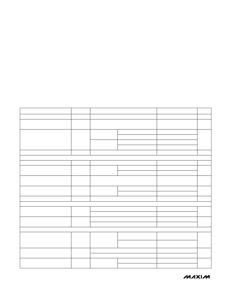
ABSOLUTE MAXIMUM RATINGS
ELECTRICAL CHARACTERISTICS
(V
IN
=
SHDN = 3V, FREQ = GND,
T
A
= 0°C to +85°C
, unless otherwise noted. Typical values are at T
A
= +25°C.)
Stresses beyond those listed under “Absolute Maximum Ratings” may cause permanent damage to the device. These are stress ratings only, and functional
operation of the device at these or any other conditions beyond those indicated in the operational sections of the specifications is not implied. Exposure to
absolute maximum rating conditions for extended periods may affect device reliability.
LX to GND ..............................................................-0.3V to +14V
IN, SHDN, FREQ, FB to GND ................................-0.3V to +6.2V
SS, COMP to GND .......................................-0.3V to (V
IN
+ 0.3V)
RMS LX Pin Current ..............................................................1.2A
Continuous Power Dissipation (T
A
= +70°C)
8-Pin µMAX (derate 4.1mW/°C above +70°C) .............330mW
Operating Temperature Range
MAX1790EUA/MAX8715EUA ........................-40°C to +85°C
Junction Temperature ......................................................+150°C
Storage Temperature Range .............................-65°C to +150°C
Lead Temperature (soldering, 10s) .................................+300°C
PARAMETER
SYMBOL
CONDITIONS
MIN
TYP
MAX
UNITS
Input Supply Range
V
IN
2.6
5.5
V
V
IN
Undervoltage Lockout
UVLO
V
IN
rising, typical hysteresis is 40mV,
LX remains off below this level
2.25
2.38
2.52
V
V
FB
= 1.3V, not switching
0.18
0.35
MAX1790
V
FB
= 1.0V, switching
2
5
V
FB
= 1.3V, not switching
0.21
0.35
Quiescent Current
I
IN
MAX8715
V
FB
= 1.0V, switching
2.5
5.0
mA
Shutdown Supply Current
I
IN
SHDN = GND
0.1
10
µA
ERROR AMPLIFIER
Feedback Voltage
V
FB
Level to produce V
COMP
= 1.24V
1.222
1.24
1.258
V
MAX1790
0
40
FB Input Bias Current
I
FB
V
FB
= 1.24V
MAX8715
125
190
nA
Feedback-Voltage Line
Regulation
Level to produce V
COMP
= 1.24V,
2.6V < V
IN
< 5.5V
0.05
0.15
%/V
MAX1790
70
140
240
Transconductance
g
m
∆I = 5µA
MAX8715
70
160
240
µS
Voltage Gain
A
V
700
V/V
OSCILLATOR
FREQ = GND
540
640
740
Frequency
f
OSC
FREQ = IN
1000
1220
1500
kHz
FREQ = GND
79
85
92
Maximum Duty Cycle
DC
FREQ = IN
84
%
N-CHANNEL SWITCH
MAX1790
1.2
1.6
2.3
Current Limit
I
LIM
V
FB
= 1V,
duty cycle =
65% (Note 1)
MAX8715
1.8
2.4
3.4
A
MAX1790
0.21
0.5
On-Resistance
R
ON
MAX8715
0.15
0.35
Ω
MAX1790
0.01
20
Leakage Current
I
LXOFF
V
LX
= 12V
MAX8715
5
30
µA