Chip information, Layout procedure – Rainbow Electronics MAX8715 User Manual
Page 13
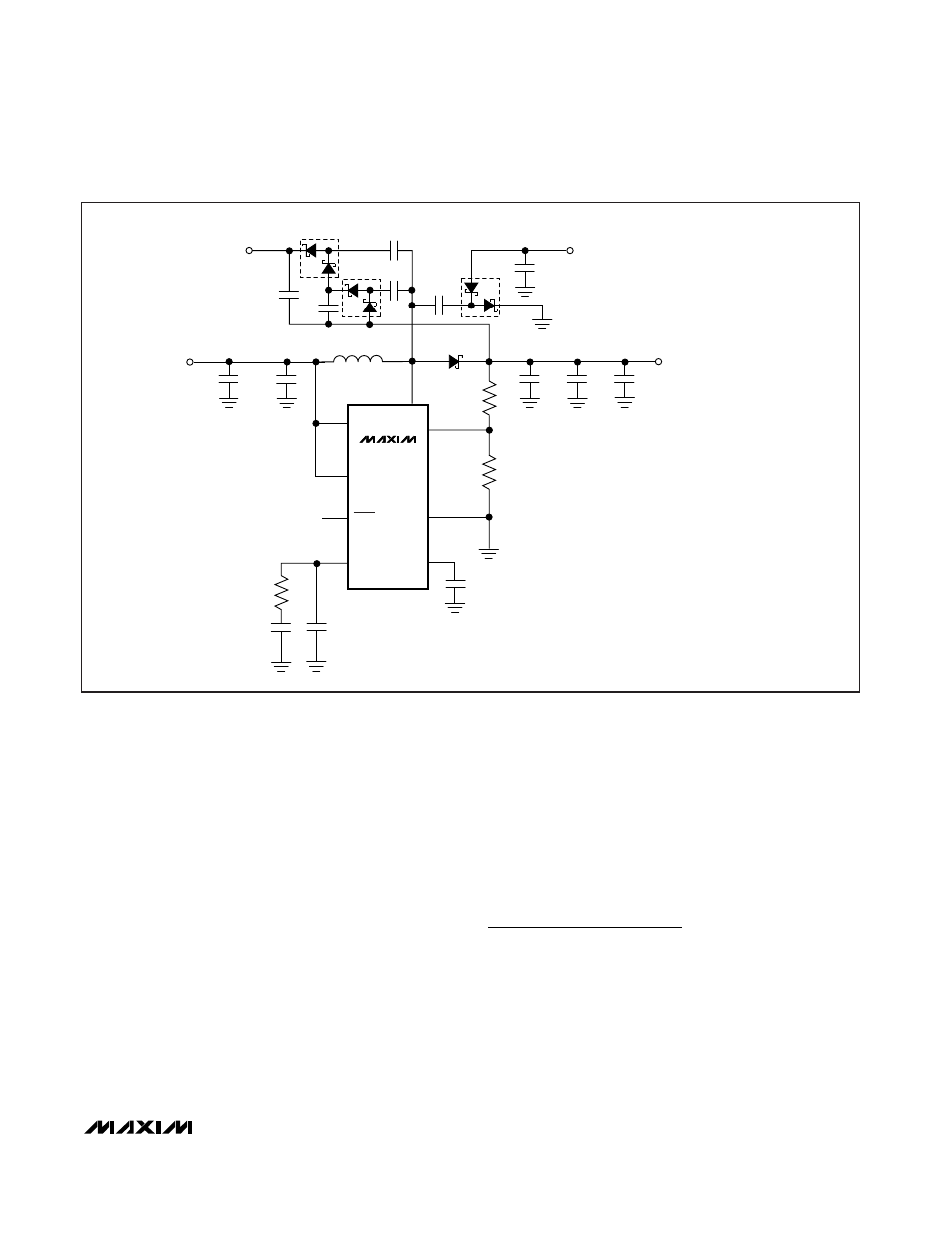
AMLCD Application
Figure 4 shows a power supply for active matrix (TFT-
LCD) flat-panel displays. Output-voltage transient per-
formance is a function of the load characteristic. Add or
remove output capacitance (and recalculate compen-
sation-network component values) as necessary to
meet transient performance. Regulation performance
for secondary outputs (V2 and V3) depends on the load
characteristics of all three outputs.
Layout Procedure
Good PC board layout and routing are required in high-
frequency switching power supplies to achieve good reg-
ulation, high efficiency, and stability. It is strongly recom-
mended that the evaluation kit PC board layouts be fol-
lowed as closely as possible. Place power components
as close together as possible, keeping their traces short,
direct, and wide. Avoid interconnecting the ground pins
of the power components using vias through an internal
ground plane. Instead, keep the power components
close together and route them in a star ground configura-
tion using component-side copper, then connect the star
ground to internal ground using multiple vias.
Chip Information
TRANSISTOR COUNT: 1012
MAX1790/MAX8715
Low-Noise Step-Up DC-DC Converters
______________________________________________________________________________________
13
Figure 4. Multiple-Output, Low-Profile (1.2mm max) TFT-LCD Power Supply
FB
LX
GND
18pF (MAX1790)
10pF (MAX8715)
27nF
C1, C2, C3, C4: TAIYO YUDEN LMK325BJ335MD (3.3
µF, 10V)
D1: ZETEX ZHCS1000 (20V, 1A, SCHOTTKY) OR MOTOROLA MBRM120ET3
D2, D3, D4: ZETEX BAT54S (30V, 200mA, SCHOTTKY)
L1: SUMIDA CLQ4D10-6R8 (6.8
µH, 0.8A) OR SUMITOMO CXLM120-6R8
274k
Ω
44.2k
Ω
FREQ
IN
3.0V TO 3.6V
V2
+26V
5mA
V1
9V
150mA
V3
-9V
10mA
COMP
SHDN
SS
D1
D2
D3
D4
0.47
µF
1
µF
1
µF
1
µF
0.1
µF
0.1
µF
MAX1790
MAX8715
470pF (MAX1790)
750pF (MAX8715)
150k
Ω (MAX1790)
82k
Ω (MAX8715)
C1
C3
C2
3.3
µF
C4
L1