Rainbow Electronics MAX8715 User Manual
Page 12
MAX1790/MAX8715
Low-Noise Step-Up DC-DC Converters
12
______________________________________________________________________________________
R2 can have a value up to 100k
Ω without sacrificing
accuracy. Connect the resistor-divider as close to the IC
as possible.
Loop Compensation
The voltage feedback loop needs proper compensation
to prevent excessive output ripple and poor efficiency
caused by instability. This is done by connecting a resis-
tor (R
COMP
) and capacitor (C
COMP
) in series from
COMP to GND, and another capacitor (C
COMP2
) from
COMP to GND. R
COMP
is chosen to set the high-fre-
quency integrator gain for fast transient response, while
C
COMP
is chosen to set the integrator zero to maintain
loop stability. The second capacitor, C
COMP2
, is chosen
to cancel the zero introduced by output-capacitance
ESR. For optimal performance, choose the components
using the following equations:
R
COMP
≅ (200Ω / A
2
) x V
OUT2
x C
OUT
/ L (MAX1790)
R
COMP
≅ (274Ω / A) x V
IN
x V
OUT
x C
OUT
/ (L x I
OUT
)
(MAX8715)
C
COMP
≅ (0.4 x 10
-3
A/
Ω) x L / V
IN
(MAX1790)
C
COMP
≅ (0.36 x 10
-3
A/
Ω) x L / V
IN
(MAX8715)
C
COMP2
≅ (0.005 A
2
/
Ω) x R
ESR
x L / V
OUT2
(MAX1790)
C
COMP2
≅ (0.0036 A/Ω) x R
ESR
x L x I
OUT / (VIN
x
VOUT)
(MAX8715)
For the ceramic output capacitor, where ESR is small,
C
COMP2
is optional. Table 1 shows experimentally verified
external component values for several applications.
The best gauge of correct loop compensation is by
inspecting the transient response of the MAX1790/
MAX8715. Adjust R
COMP
and C
COMP
as necessary to
obtain optimal transient performance.
Soft-Start Capacitor
The soft-start capacitor should be large enough that it
does not reach final value before the output has
reached regulation. Calculate C
SS
to be:
where:
C
OUT
= total output capacitance including any bypass
capacitor on the output bus
V
OUT
= maximum output voltage
I
INRUSH
= peak inrush current allowed
I
OUT
= maximum output current during power-up stage
V
IN
= minimum input voltage
The load must wait for the soft-start cycle to finish
before drawing a significant amount of load current.
The duration after which the load can begin to draw
maximum load current is:
t
MAX
= 6.77 x 10
5
C
SS
Application Circuits
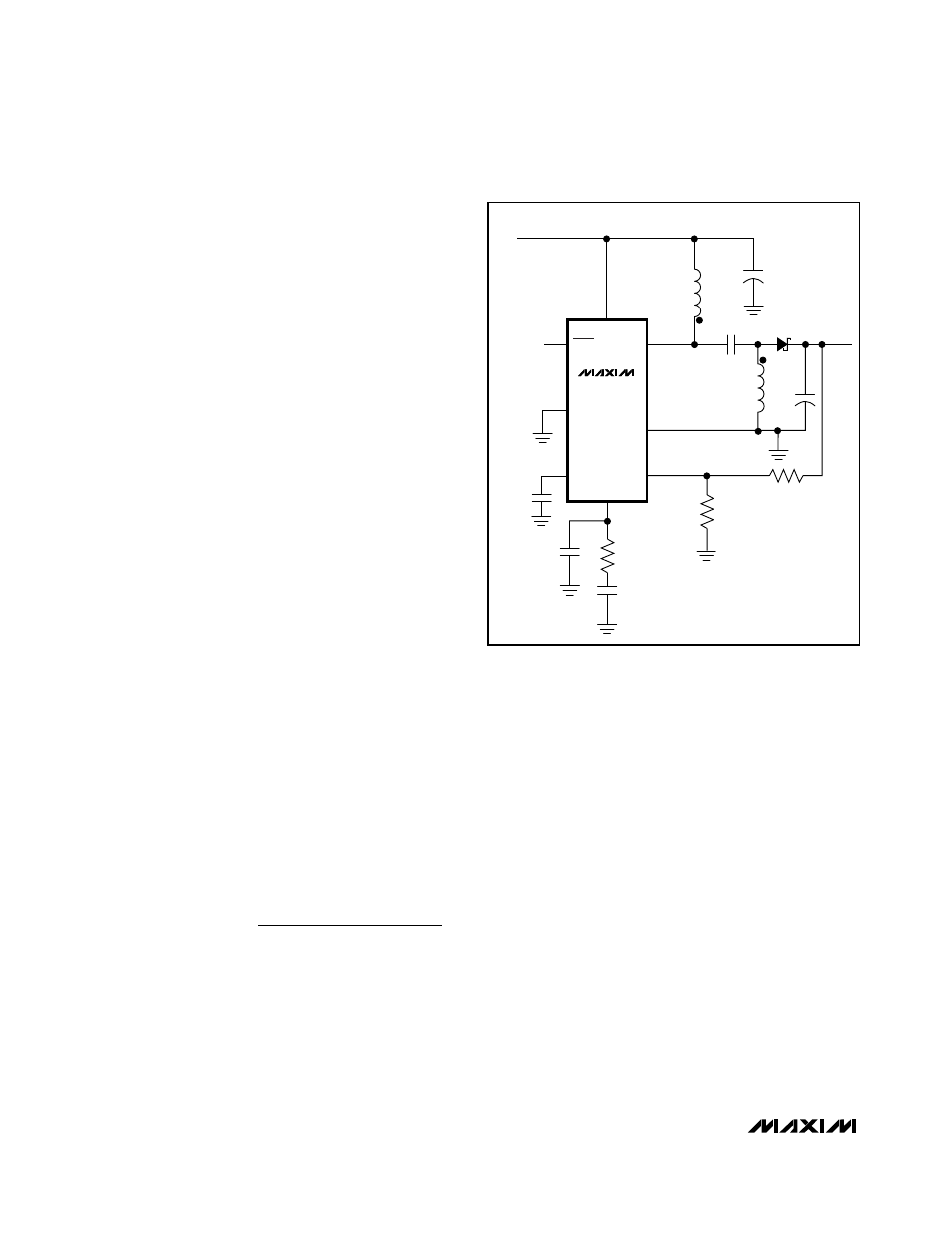
1-Cell to 3.3V SEPIC Power Supply
Figure 3 shows the MAX1790 in a single-ended primary
inductance converter (SEPIC) topology. This topology is
useful when the input voltage can be either higher or
lower than the output voltage, such as when converting
a single lithium-ion (Li+) cell to a 3.3V output. L1A and
L1B are two windings on a single inductor. The coupling
capacitor between these two windings must be a low-
ESR type to achieve maximum efficiency, and must also
be able to handle high ripple currents. Ceramic capaci-
tors are best for this application. The circuit in Figure 3
provides 400mA output current at 3.3V output when
operating with an input voltage from +2.6V to +5.5V.
C
21
10
C
V
V
V
V
I
I
V
SS
6
OUT
IN
OUT
IN
INRUSH
OUT
OUT
OUT
2
>
Ч
Ч
−
Ч
Ч
−
Ч
⎛
⎝
⎜
⎞
⎠
⎟
−
LX
IN
V
IN
2.6V TO 5.5V
GND
L1 = CTX8-1P
C
OUT
= TPSD226025R0200
C2
10
µF
FREQ
V
OUT
3.3V
CC
SS
SHDN
FB
D1
R1
1M
Ω
R2
605k
Ω
L1A
5.3
µH
0.027
µF
MAX1790
C
OUT
22
µF
20V
C1
10
µF
10V
R
COMP
22k
Ω
C
COMP
330pF
C
COMP2
56pF
L1B
5.3
µH
Figure 3. MAX1790 in a SEPIC Configuration