Rainbow Electronics MAX2051 User Manual
Page 13
MAX2051
SiGe, High-Linearity, 850MHz to 1550MHz
Up/Downconversion Mixer with LO Buffer
______________________________________________________________________________________
13
Pin Description
Typical Operating Characteristics (continued)
(
Typical Application Circuit, Upconversion mode, V
CC
= +5.0V, P
LO
= 0dBm, P
IF
= 0dBm, f
IF
= 350MHz, LO is high-side injected,
T
C
=+25°C, unless otherwise noted.)
PIN
NAME
FUNCTION
1
RF
Single-Ended 50
Ω RF Input. Internally matched and DC shorted to GND through a balun. Requires
an input DC-blocking capacitor.
2–5, 9, 10, 11,
13, 14
GND
Ground. Internally connected to the exposed pad. Connect all ground pins and the exposed pad
(EP) together.
6, 8, 15
V
CC
Power Supply. Bypass to GND with capacitors as close as possible to the pin (see the Typical
Application Circuit).
7
LOBIAS
LO Amplifier Bias Control. Output bias resistor for the LO buffer. Connect a 61.9
Ω ±1% resistor
from LOBIAS to V
CC
to set the bias current for the main LO amplifier.
12
LO
Local Oscillator Input. This input is internally matched to 50
Ω. Requires an input DC-blocking
capacitor.
16, 17
IF+, IF-
Differential IF Output
18, 19, 20
GND
Ground. Not internally connected. Ground these pins or leave unconnected.
—
EP
Exposed Pad. Internally connected to GND. Solder this exposed pad to a PCB pad that uses
multiple ground vias to provide heat transfer out of the device into the PCB ground planes. These
multiple ground vias are also required to achieve the noted RF performance.
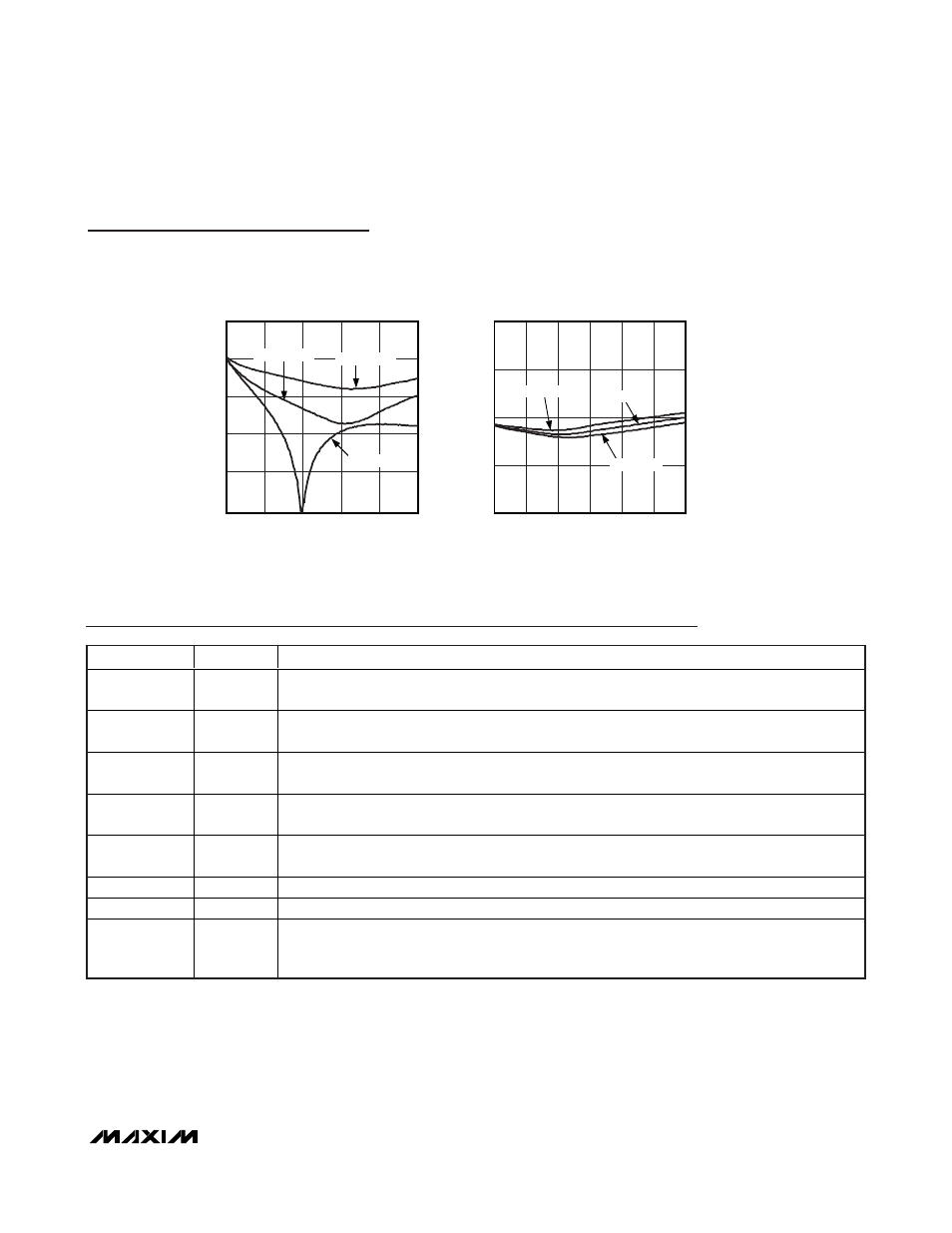
MAX2051 toc62
50
20
30
40
10
0
320
230
140
50
410
500
IF PORT RETURN LOSS vs. IF FREQUENCY
(UPCONVERSION MODE)
IF FREQUENCY (MHz)
IF PORT RETURN LOSS (dB)
f
LO
= 1200MHz
f
LO
= 1500MHz
f
LO
= 1900MHz
MAX2051 toc63
1850
1700
1550
1400
10
15
5
0
20
1100
1250
2000
LO RETURN LOSS vs. LO FREQUENCY
(UPCONVERSION MODE)
LO FREQUENCY (MHz)
LO RETURN LOSS (dB)
P
LO
= +3dBm
P
LO
= 0dBm
P
LO
= -3dBm