Table 3. output voltage programming – Rainbow Electronics MAX1842 User Manual
Page 12
MAX1742/MAX1842
1A/2.7A, 1MHz, Step-Down Regulators with
Synchronous Rectification and Internal Switches
12
______________________________________________________________________________________
2) Select the constant off-time as a function of input
voltage, output voltage, and switching frequency.
3) Select R
TOFF
as a function of off-time.
4) Select the inductor as a function of output voltage,
off-time, and peak-to-peak inductor current.
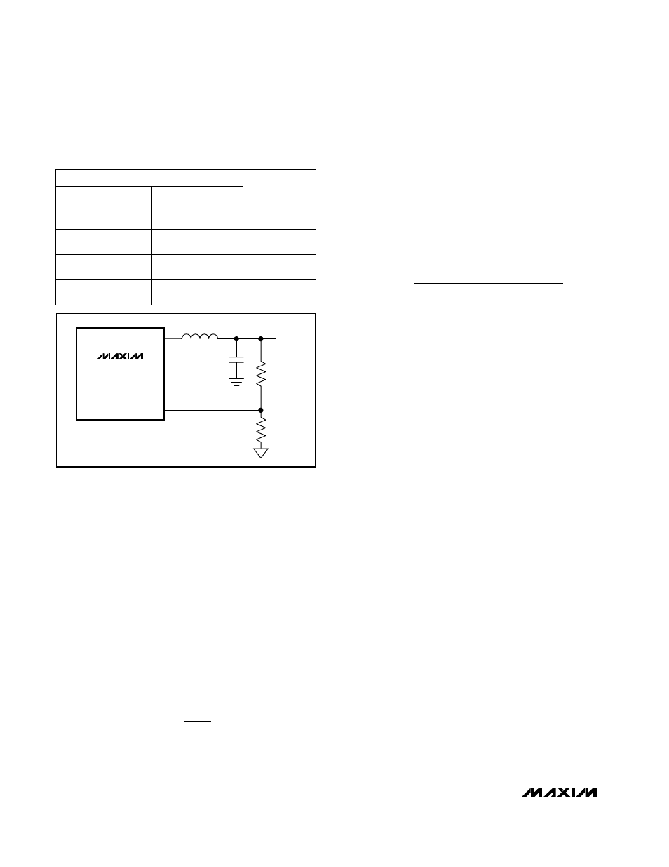
Setting the Output Voltage
The output of the MAX1742/MAX1842 is selectable
between one of three preset output voltages: 2.5V,
1.8V, and 1.5V. For a preset output voltage, connect FB
to the output voltage and connect FBSEL as indicated
in Table 3. For an adjustable output voltage, connect
FBSEL to GND and connect FB to a resistive divider
between the output voltage and ground (Figure 4).
Regulation is maintained for adjustable output voltages
when V
FB
= V
REF
. Use 50k
Ω for R1. R2 is given by the
equation:
where V
REF
is typically 1.1V.
Programming the Switching Frequency
and Off-Time
The MAX1742/MAX1842 features a programmable
PWM mode switching frequency, which is set by the
input and output voltage and the value of R
TOFF
, con-
nected from TOFF to GND. R
TOFF
sets the PMOS
power switch off-time in PWM mode. Use the following
equation to select the off-time according to your
desired switching frequency in PWM mode:
where:
t
OFF
= the programmed off-time
V
IN
= the input voltage
V
OUT
= the output voltage
V
PMOS
= the voltage drop across the internal
PMOS power switch
V
NMOS
= the voltage drop across the internal
NMOS synchronous-rectifier switch
f
PWM
= switching frequency in PWM mode
Select R
TOFF
according to the formula:
R
TOFF
= (t
OFF
- 0.07µs) (110k
Ω / 1.00µs)
Recommended values for R
TOFF
range from 36k
Ω to
430k
Ω for off-times of 0.4µs to 4µs.
Inductor Selection
The key inductor parameters must be specified: inductor
value (L) and peak current (I
PEAK
). The following equa-
tion includes a constant, denoted as LIR, which is the
ratio of peak-to-peak inductor AC current (ripple current)
to maximum DC load current. A higher value of LIR allows
smaller inductance but results in higher losses and ripple.
A good compromise between size and losses is found at
approximately a 25% ripple-current to load-current ratio
(LIR = 0.25), which corresponds to a peak inductor cur-
rent 1.125 times the DC load current:
where: I
OUT
= maximum DC load current
LIR = ratio of peak-to-peak AC inductor current
to DC load current, typically 0.25
L
V
t
I
LIR
OUT
OFF
OUT
=
Ч
Ч
t
V
V
V
f
V
V
V
OFF
IN
OUT
PMOS
PWM
IN
PMOS
NMOS
–
=
−
(
)
−
+
(
)
R2
R1
V
V
1
OUT
REF
=
−
Figure 4. Adjustable Output Voltage
PIN
2.5
V
CC
Output voltage
1.5
1.8
REF
Output voltage
Adjustable
GND
Resistive
divider
FB
OUTPUT
VOLTAGE
(V)
FBSEL
Unconnected
Output voltage
Table 3. Output Voltage Programming
LX
R2
R1
R1 = 50k
Ω
R2 = R1(V
OUT
/ V
REF
- 1)
V
REF
= 1.1V
FB
V
OUT
MAX1742
MAX1842