Design procedure – Rainbow Electronics MAX1842 User Manual
Page 11

MAX1742/MAX1842
1A/2.7A, 1MHz, Step-Down Regulators with
Synchronous Rectification and Internal Switches
______________________________________________________________________________________
11
constant-off-time mode, the synchronous-rectifier
switch turns off just prior to the PMOS power switch
turning on. While both switches are off, inductor current
flows through the internal body diode of the NMOS
switch. The internal body diode’s forward voltage is rel-
atively high.
Thermal Resistance
Junction-to-ambient thermal resistance,
θ
JA
, is highly
dependent on the amount of copper area immediately
surrounding the IC leads. The MAX1742 evaluation kit
has 0.5in
2
of copper area and a thermal resistance of
80°C/W with no forced airflow. Airflow over the board
significantly reduces the junction-to-ambient thermal
resistance. For heatsinking purposes, evenly distribute
the copper area connected at the IC among the high-
current pins.
Power Dissipation
Power dissipation in the MAX1742/MAX1842 is domi-
nated by conduction losses in the two internal power
switches. Power dissipation due to supply current in the
control section and average current used to charge
and discharge the gate capacitance of the internal
switches (i.e., switching losses) is approximately:
P
DS
= C x V
IN2
x f
PWM
where C = 2.5nF and f
PWM
is the switching frequen-
cy in PWM mode.
This number is reduced when the switching frequency
decreases as the part enters Idle Mode. Combined con-
duction losses in the two power switches are approxi-
mated by:
P
D
= I
OUT2
x R
PMOS
where R
PMOS
is the on-resistance of the PMOS switch.
The junction-to-ambient thermal resistance required to
dissipate this amount of power is calculated by:
θ
JA
= (T
J,MAX
- T
A,MAX
) / P
D(T
OT
)
where:
θ
JA
= junction-to-ambient thermal resistance
T
J,MAX
= maximum junction temperature
T
A,MAX
= maximum ambient temperature
P
D(TOT)
= total losses
__________________Design Procedure
For typical applications, use the recommended compo-
nent values in Tables 1 or 2. For other applications,
take the following steps:
1) Select the desired PWM-mode switching frequency;
1MHz is a good starting point. See Figure 3 for maxi-
mum operating frequency.
V
OUT
(V)
R
TOFF
(k
Ω)
5.6
39
L
(µH)
5
3.3
5.6
V
IN
(V)
47
5.6
75
5
1.8
3.9
39
3.3
2.5
3.9
43
3.3
1.8
3.9
56
3.3
1.5
5
2.5
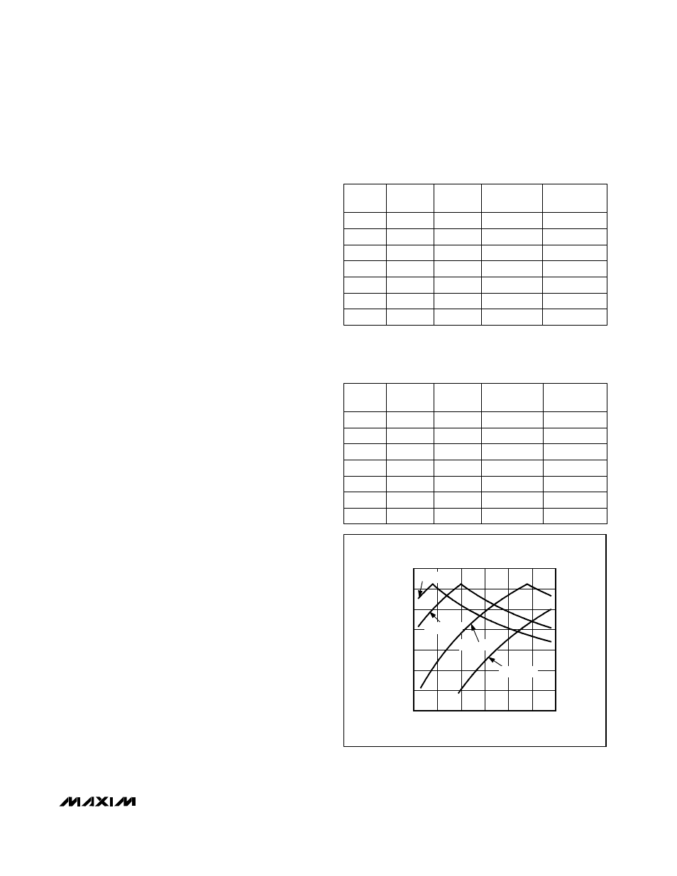
Table 1. MAX1742 Recommended
Component Values (I
OUT
= 1A)
5.6
100
5
1.5
f
PWM
(kHz)
850
910
610
1050
1000
770
1070
Table 2. MAX1842 Recommended
Component Values (Continuous Output
Current = 1A, Burst Output Current = 2.7A)
1180
715
940
985
570
850
800
f
PWM
(kHz)
1.5
5
100
2.2
2.5
5
1.5
3.3
56
1.5
1.8
3.3
43
1.5
2.5
3.3
39
1.5
1.8
5
75
2.2
47
V
IN
(V)
2.2
3.3
5
L
(µH)
39
2.2
R
TOFF
(k
Ω)
V
OUT
(V)
0
400
200
800
600
1200
1000
1400
2.6
3.6
4.1
3.1
4.6
5.1
5.6
MAXIMUM RECOMMENDED
OPERATING FREQUENCY vs. INPUT VOLTAGE
MAX1842 fig03
V
IN
(V)
OPERATING FREQUENCY (kHz)
V
OUT
= 1.5V
V
OUT
= 1.8V
V
OUT
= 2.5V
V
OUT
= 3.3V
Figure 3. Maximum Recommended Operating Frequency vs.
Input Voltage
