Detailed description, Applications information, Layout issues – Rainbow Electronics MAX2682 User Manual
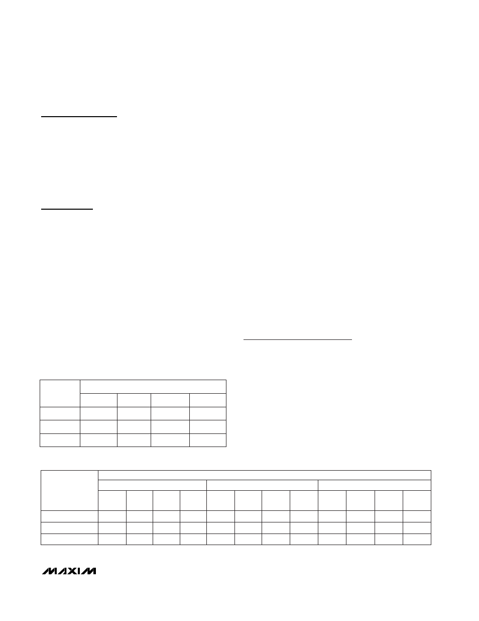
Page 9: Table 1. rfin port impedance
Detailed Description
The MAX2680/MAX2681/MAX2682 are 400MHz to
2.5GHz, silicon-germanium, double-balanced down-
converter mixers. They are designed to provide opti-
mum linearity performance for a specified supply
current. They consist of a double-balanced Gilbert-cell
mixer with single-ended RF, LO, and IF port connec-
tions. An on-chip bias cell provides a low-power shut-
down feature. Consult the
Selector Guide
for device
features and comparison.
Applications Information
Local-Oscillator (LO) Input
The LO input is a single-ended broadband port with a
typical input VSWR of better than 2.0:1 from 400MHz to
2.5GHz. The LO signal is mixed with the RF input sig-
nal, and the resulting downconverted output appears at
IFOUT. AC-couple LO with a capacitor. Drive the LO
port with a signal ranging from -10dBm to 0 (50
Ω
source).
RF Input
The RF input frequency range is 400MHz to 2.5GHz.
The RF input requires an impedance-matching network
as well as a DC-blocking capacitor that can be part of
the matching network. Consult Tables 1 and 2, as well
as the RF Port Impedance vs. RF Frequency graph in
the
Typical Operating Characteristics
for information on
matching.
IF Output
The IF output frequency range extends from 10MHz to
500MHz. IFOUT is a high-impedance, open-collector
output that requires an external inductor to V
CC
for
proper biasing. For optimum performance, the IF port
requires an impedance-matching network. The configu-
ration and values for the matching network is depen-
dent upon the frequency and desired output
impedance. For assistance in choosing components for
optimal performance, refer to Tables 3 and 4 as well as
the IF Port Impedance vs. IF Frequency graph in the
Typical Operating Characteristics.
Power-Supply and
S
SH
HD
DN
N Bypassing
Proper attention to voltage supply bypassing is essen-
tial for high-frequency RF circuit stability. Bypass V
CC
with a 10µF capacitor in parallel with a 1000pF capaci-
tor. Use separate vias to the ground plane for each of
the bypass capacitors and minimize trace length to
reduce inductance. Use separate vias to the ground
plane for each ground pin. Use low-inductance ground
connections.
Decouple SHDN with a 1000pF capacitor to ground to
minimize noise on the internal bias cell. Use a series
resistor (typically 100
Ω
) to reduce coupling of high-fre-
quency signals into the SHDN pin.
Layout Issues
A well designed PC board is an essential part of an RF
circuit. For best performance, pay attention to power-
supply issues as well as to the layout of the RFIN and
IFOUT impedance-matching network.
MAX2680/MAX2681/MAX2682
400MHz to 2.5GHz, Low-Noise,
SiGe Downconverter Mixers
_______________________________________________________________________________________
9
179-j356
MAX2680
Table 1. RFIN Port Impedance
54-j179
32-j94
33-j73
FREQUENCY
75-j188
209-j332
MAX2681
34-j108
33-j86
78-j182
206-j306
MAX2682
34-j106
29-j86
Table 2. RF Input Impedance-Matching Component Values
270pF
86nH
Z1
1.5pF
Short
MAX2680
22nH
270pF
Z2
270pF
270pF
Open
Open
Z3
1.8nH
1.8nH
Note:
Z1, Z2, and Z3 are found in the Typical Operating Circuit.
270pF
68nH
1.5pF
Short
MAX2681
18nH
270pF
270pF
270pF
Open
0.5pF
1.8nH
2.2nH
1.5pF
68nH
Short
Short
MAX2682
270pF
270pF
270pF
270pF
10nH
0.5pF
2.2nH
1.2nH
900
MHz
1950
MHz
2450
MHz
900
MHz
1950
MHz
2450
MHz
400
MHz
900
MHz
1950
MHz
400
MHz
2450
MHz
400
MHz
900MHz
1950MHz
2450MHz
PART
400MHz
FREQUENCY
MATCHING
COMPONENTS