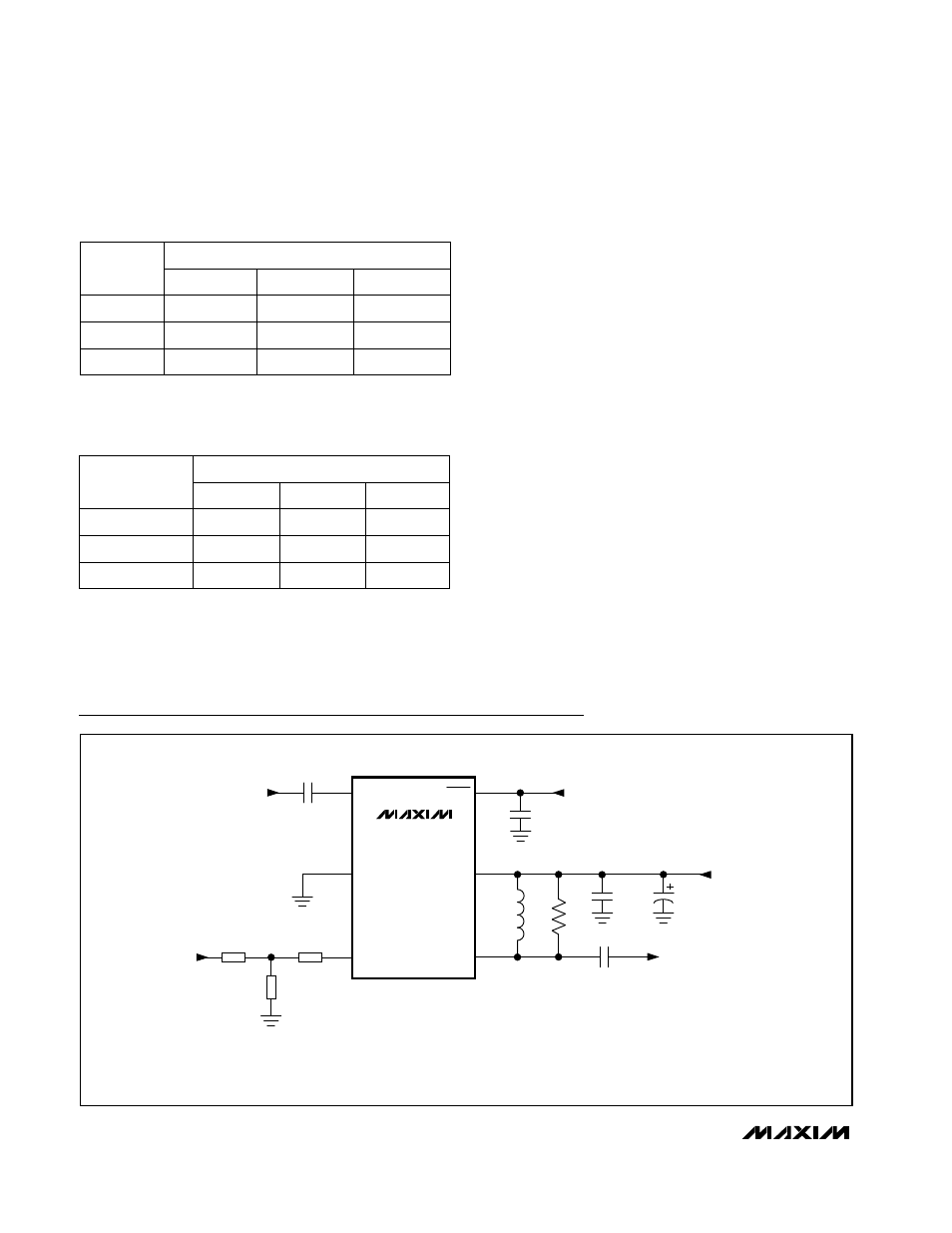
Typical operating circuit, Table 3. ifout port impedance, Table 4. if output impedance-matching components – Rainbow Electronics MAX2682 User Manual
Page 10: Power-supply layout, Impedance-matching network layout

MAX2680/MAX2681/MAX2682
Power-Supply Layout
To minimize coupling between different sections of the
IC, the ideal power-supply layout is a star configuration
with a large decoupling capacitor at a central V
CC
node. The V
CC
traces branch out from this central
node, each going to a separate V
CC
node on the PC
board. At the end of each trace is a bypass capacitor
that has low ESR at the RF frequency of operation. This
arrangement provides local decoupling at the V
CC
pin.
At high frequencies, any signal leaking out of one sup-
ply pin sees a relatively high impedance (formed by the
V
CC
trace inductance) to the central V
CC
node, and an
even higher impedance to any other supply pin, as well
as a low impedance to ground through the bypass
capacitor.
Impedance-Matching Network Layout
The RFIN and IFOUT impedance-matching networks are
very sensitive to layout-related parasitics. To minimize
parasitic inductance, keep all traces short and place
components as close as possible to the chip. To mini-
mize parasitic capacitance, use cutouts in the ground
plane (and any other plane) below the matching network
components. However, avoid cutouts that are larger
than necessary since they act as aperture antennas.
400MHz to 2.5GHz, Low-Noise,
SiGe Downconverter Mixers
10
______________________________________________________________________________________
Table 3. IFOUT Port Impedance
803-j785
960-j372
MAX2680
186-j397
FREQUENCY
746-j526
934-j373
MAX2681
161-j375
578-j299
670-j216
MAX2682
175-j296
Table 4. IF Output Impedance-Matching
Components
330nH
390nH
L1
82nH
FREQUENCY
15pF
39pF
C2
3pF
Open
250
Ω
R1
Open
70MHz
240MHz
PART
45MHz
70MHz
240MHz
MATCHING
COMPONENT
45MHz
MAX2680
MAX2681
MAX2682
LO
C3
6
5
4
SHUTDOWN
CONTROL
1
SHDN
V
CC
RF
INPUT
LO
INPUT
C1
IFOUT
2
Z
2
Z
3
Z
1
3
GND
RFIN
THE VALUES OF MATCHING COMPONENTS C2, L1, R1, Z1, Z2, AND Z3 DEPEND ON THE IF AND RF FREQUENCY AND DOWNCONVERTER. SEE TABLES 2 AND 4.
V
CC
+2.7V TO +5.5V
IF
OUTPUT
L1
C2
R1
C4
1000pF
C5
10
µ
F
Typical Operating Circuit
